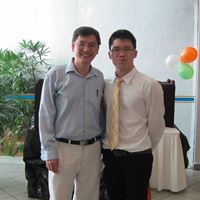
Changhua Chen
age ~44
from San Ramon, CA
- Also known as:
-
- Hua Chen Chang
Changhua Chen Phones & Addresses
- San Ramon, CA
- Danville, CA
- Davis, CA
Us Patents
-
Epitaxial Material Grown Laterally Within A Trench And Method For Producing Same
view source -
US Patent:6500257, Dec 31, 2002
-
Filed:Apr 17, 1998
-
Appl. No.:09/062028
-
Inventors:Shih-Yuan Wang - Palo Alto CA
Changhua Chen - San Jose CA
Yong Chen - Mountain View CA
Scott W. Corzine - Sunnyvale CA
R. Scott Kern - San Jose CA -
Assignee:Agilent Technologies, Inc. - Palo Alto CA
-
International Classification:C30B 2300
-
US Classification:117 95, 438479
-
Abstract:An epitaxial material grown laterally in a trench allows for the fabrication of a trench-based semiconductor material that is substantially low in dislocation density. Initiating the growth from a sidewall of a trench minimizes the density of dislocations present in the lattice growth template, which minimizes the dislocation density in the regrown material. Also, by allowing the regrowth to fill and overflow the trench, the low dislocation density material can cover the entire surface of the substrate upon which the low dislocation density material is grown. Furthermore, with successive iterations of the trench growth procedure, higher quality material can be obtained. Devices that require a stable, high quality epitaxial material can then be fabricated from the low dislocation density material.
-
Formation Of Ohmic Contacts In Iii-Nitride Light Emitting Devices
view source -
US Patent:6914272, Jul 5, 2005
-
Filed:Nov 24, 2003
-
Appl. No.:10/721440
-
Inventors:Werner K. Goetz - Palo Alto CA, US
Michael D. Camras - Sunnyvale CA, US
Changhua Chen - San Jose CA, US
Gina L. Christenson - Sunnyvale CA, US
R. Scott Kern - San Jose CA, US
Chihping Kuo - Milpitas CA, US
Paul Scott Martin - Pleasanton CA, US
Daniel A. Steigerwald - Cupertino CA, US -
Assignee:Lumileds Lighting U.S., LLC - San Jose CA
-
International Classification:H01L033/00
-
US Classification:257123, 257 79, 257 86, 257102, 257103, 313506
-
Abstract:P-type layers of a GaN based light-emitting device are optimized for formation of Ohmic contact with metal. In a first embodiment, a p-type GaN transition layer with a resistivity greater than or equal to about 7 Ωcm is formed between a p-type conductivity layer and a metal contact. In a second embodiment, the p-type transition layer is any III-V semiconductor. In a third embodiment, the p-type transition layer is a superlattice. In a fourth embodiment, a single p-type layer of varying composition and varying concentration of dopant is formed.
-
Formation Of Ohmic Contacts In Iii-Nitride Light Emitting Devices
view source -
US Patent:20020008243, Jan 24, 2002
-
Filed:Jan 5, 2001
-
Appl. No.:09/755935
-
Inventors:Werner Goetz - Palo Alto CA, US
Michael Camras - Sunnyvale CA, US
Changhua Chen - San Jose CA, US
Xiaoping Chen - San Jose CA, US
Gina Christenson - Sunnyvale CA, US
R. Kern - San Jose CA, US
Chihping Kuo - Milpitas CA, US
Paul Martin - Pleasanton CA, US
Daniel Steigerwald - Cupertino CA, US -
International Classification:H01L027/15
-
US Classification:257/079000
-
Abstract:P-type layers of a GaN based light-emitting device are optimized for formation of Ohmic contact with metal. In a first embodiment, a p-type GaN transition layer with a resistivity greater than or equal to about 7 cm is formed between a p-type conductivity layer and a metal contact. In a second embodiment, the p-type transition layer is any III-V semiconductor. In a third embodiment, the p-type transition layer is a superlattice. In a fourth embodiment, a single p-type layer of varying composition and varying concentration of dopant is formed.
-
Formation Of Ohmic Contacts In Iii-Nitride Light Emitting Devices
view source -
US Patent:20050167693, Aug 4, 2005
-
Filed:Mar 30, 2005
-
Appl. No.:11/095854
-
Inventors:Werner Goetz - Palo Alto CA, US
Michael Camras - Sunnyvale CA, US
Changhua Chen - San Jose CA, US
Xiaoping Chen - San Jose CA, US
Gina Christenson - Sunnyvale CA, US
R. Kern - San Jose CA, US
Chihping Kuo - Milpitas CA, US
Paul Martin - Pleasanton CA, US
Daniel Steigerwald - Cupertino CA, US -
International Classification:H01L021/00
H01L033/00 -
US Classification:257103000, 438022000
-
Abstract:P-type layers of a GaN based light-emitting device are optimized for formation of Ohmic contact with metal. In a first embodiment, a p-type GaN transition layer with a resistivity greater than or equal to about 7 Ω cm is formed between a p-type conductivity layer and a metal contact. In a second embodiment, the p-type transition layer is any III-V semiconductor. In a third embodiment, the p-type transition layer is a superlattice. In a fourth embodiment, a single p-type layer of varying composition and varying concentration of dopant is formed.
Resumes

Changhua Chen
view source
Changhua Chen
view source
Chen Changhua
view source
Changhua Chen
view source
Derek Chen Changhua
view sourceFriends:
Zhang Ziqiang, Darryl Chan, Jennifer Tay Peiyu, Defeng Lin, Tan Zhen Hui
Youtube
Googleplus

Changhua Chen
Get Report for Changhua Chen from San Ramon, CA, age ~44


