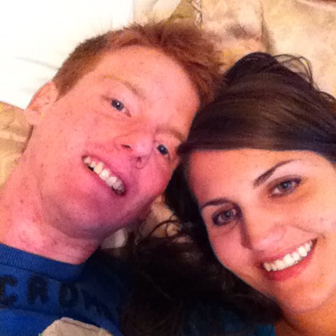
Christopher Michael Kirby
age ~43
from Dundalk, MD
- Also known as:
-
- Christopher M Kirby
- Michael Christopher Kirby
- Chris Kirby
- Christoph Kirby
- Christophe Kirby
- Phone and address:
-
8113 Del Haven Rd, Baltimore, MD 21222
4102881565
Christopher Kirby Phones & Addresses
- 8113 Del Haven Rd, Dundalk, MD 21222 • 4102881565
- Baltimore, MD
- Marion, SC
Work
-
Company:Metro practice mgmt group
-
Address:8630 Fenton Street, Silver Spring, MD 20910
-
Phones:3015652250
-
Position:Ceo
-
Industries:Industrial and Commercial Machinery and Equipment
Lawyers & Attorneys

Christopher Kirby - Lawyer
view sourceOffice:
The Scher Law Firm, LLP
Specialties:
Juvenile
Construction Law
Labor Law
Employment Law
Construction Law
Labor Law
Employment Law
ISLN:
921163709
Admitted:
1997
University:
University of Texas at Austin, B.A., 1993
Law School:
Benjamin N. Cardozo School of Law, Yeshiva University, J.D., 1997

Christopher Kirby - Lawyer
view sourceOffice:
Enoch Kever PLLC
ISLN:
1000879074
Admitted:
2019
Law School:
University of Texas School of Law, Doctor of Jurisprudence/Juris Doctor (J.D.), 2019
Resumes

Christopher Kirby
view sourceLocation:
United States

Christopher Kirby
view sourceLocation:
United States

It Consultant
view sourcePosition:
consultant at Consultant
Location:
Baltimore, Maryland Area
Industry:
Computer Software
Work:
Consultant since Jan 2010
consultant
Raptor Trading Systems 2008 - 2009
Systems Analyst
consultant
Raptor Trading Systems 2008 - 2009
Systems Analyst

Christopher Kirby Baltimore, MD
view sourceWork:
Firvida
Tysons Corner, VA
May 2011 to Jan 2014
Construction Worker Metro staffing
Baltimore, MD
May 2001 to Apr 2010
Forklift Operator
Tysons Corner, VA
May 2011 to Jan 2014
Construction Worker Metro staffing
Baltimore, MD
May 2001 to Apr 2010
Forklift Operator

Christopher Kirby Baltimore, MD
view sourceWork:
BP PACKAGING
Jan 2005 to 2000
Forklift, Shipping and Receiving, UPS World Ship, fed-ex, data entry Restoration Hardware
Baltimore, MD
Nov 2003 to Dec 2005
Forklift Driver Cavanaugh Press
Baltimore, MD
Aug 2000 to Sep 2003
Bindery Production Worker
Jan 2005 to 2000
Forklift, Shipping and Receiving, UPS World Ship, fed-ex, data entry Restoration Hardware
Baltimore, MD
Nov 2003 to Dec 2005
Forklift Driver Cavanaugh Press
Baltimore, MD
Aug 2000 to Sep 2003
Bindery Production Worker
Education:
Overlea High School
Baltimore, MD
2000
Diploma in Graphic Technology
Baltimore, MD
2000
Diploma in Graphic Technology
Name / Title
Company / Classification
Phones & Addresses
CEO
Metro Practice Mgmt Group
Industrial and Commercial Machinery and Equip...
Industrial and Commercial Machinery and Equip...
8630 Fenton Street, Silver Spring, MD 20910
KIRBY BROTHERS EXCAVTING INC
UBERPOWER, LC
Director
Pedernales River Fellowship
Membership Organization
Membership Organization
Us Patents
-
Low Charging Dielectric For Capacitive Mems Devices And Method Of Making Same
view source -
US Patent:20060138604, Jun 29, 2006
-
Filed:Dec 27, 2004
-
Appl. No.:11/020270
-
Inventors:Christopher Kirby - Gambrills MD, US
Robert Horner - Severn MD, US
Harlan Cramer - Columbia MD, US
Robert Howell - Silver Spring MD, US
Robert Tranchini - Ellicott City MD, US
Gregory DeSalvo - Joppa MD, US
Gilbert Dix - Annapolis MD, US
Jeremiah Horner - Glen Burnie MD, US -
Assignee:NORTHROP GRUMMAN CORPORATION - Los Angles CA
-
International Classification:H01L 23/58
-
US Classification:257640000
-
Abstract:An improved dielectric suitable for use in electronic and micro-electromechanical (MEMS) components. The dielectric includes silicon nitride having a percentage of Si:H bonds greater than a percentage of N:H bonds, in order to reduce the level of charge trapping of the silicon nitride.
-
Infrared Multiplier For Photo-Conducting Sensors
view source -
US Patent:20140061833, Mar 6, 2014
-
Filed:Sep 5, 2012
-
Appl. No.:13/603788
-
Inventors:Thomas J. Knight - Silver Spring MD, US
Christopher F. Kirby - Gambrills MD, US -
Assignee:NORTHROP GRUMMAN SYSTEMS CORPORATION - Los Angeles CA
-
International Classification:H01L 31/0232
H01L 27/144 -
US Classification:257432, 257E31127, 257E27127
-
Abstract:Photo-conducting infrared sensors are provided including a substrate (e.g., silicon) with one or more trenches formed on a first surface. An infrared-reflective film can be deposited directly or indirectly onto and conforming in shape with the first surface of the substrate. A lead chalcogenide film can be deposited directly or indirectly over the top of the infrared-reflective film and conforming in shape with the first surface of the substrate. Accordingly, the infrared-reflective film is directly or indirectly sandwiched between the substrate and the lead chalcogenide film.
-
Preclean And Dielectric Deposition Methodology For Superconductor Interconnect Fabrication
view source -
US Patent:20200144114, May 7, 2020
-
Filed:Nov 1, 2018
-
Appl. No.:16/178306
-
Inventors:BRIAN PAUL WAGNER - BALTIMORE MD, US
CHRISTOPHER F. KIRBY - GAMBRILLS MD, US
MICHAEL RENNIE - ASHLAND VA, US
JAMES T. KELLIHER - ELKRIDGE MD, US -
Assignee:NORTHROP GRUMMAN SYSTEMS CORPORATION - FALLS CHURCH VA
-
International Classification:H01L 21/768
H01L 23/532
H01L 21/02 -
Abstract:A method is provided of forming a superconductor device interconnect structure. The method comprises forming a first dielectric layer overlying a substrate and forming a superconducting interconnect element in the first dielectric layer. The superconducting interconnect element includes a top surface aligned with a top surface of the first dielectric layer to form a first interconnect layer. The superconductor device interconnect structure is moved into a dielectric deposition chamber. The method further comprises performing a cleaning process on a top surface of the first interconnect layer in the dielectric deposition chamber to remove oxidization from a top surface of the first interconnect layer, and depositing a second dielectric layer over the first interconnect layer in the dielectric deposition chamber.
-
Deposition Methodology For Superconductor Interconnects
view source -
US Patent:20180351072, Dec 6, 2018
-
Filed:Jun 2, 2017
-
Appl. No.:15/612326
-
Inventors:CHRISTOPHER F. KIRBY - GAMBRILLS MD, US
VIVIEN M. LUU - LINTHICUM MD, US
MICHAEL RENNIE - ASHLAND VA, US
SEAN R. MCLAUGHLIN - SEVERN MD, US -
Assignee:NORTHROP GRUMMAN SYSTEMS CORPORATION - FALLS CHURCH VA
-
International Classification:H01L 39/24
H01L 21/768
H01L 21/02
H01L 23/522
H01L 23/532 -
Abstract:A method of forming a superconductor interconnect structure is disclosed. The method includes forming a dielectric layer overlying a substrate, forming an interconnect opening in the dielectric layer, and moving the substrate to a deposition chamber. The method further includes depositing a superconducting metal in the interconnect opening, by performing a series of superconducting deposition and cooling processes to maintain a chamber temperature at or below a predetermined temperature until the superconducting metal has a desired thickness, to form a superconducting element in the superconductor interconnect structure.
-
Preclean And Deposition Methodology For Superconductor Interconnects
view source -
US Patent:20180337138, Nov 22, 2018
-
Filed:May 17, 2017
-
Appl. No.:15/597565
-
Inventors:VIVIEN LUU - LINTHICUM MD, US
CHRISTOPHER F. KIRBY - GAMBRILLS MD, US
BRIAN WAGNER - BALTIMORE MD, US
MICHAEL RENNIE - ASHLAND VA, US -
Assignee:NORTHROP GRUMMAN SYSTEMS CORPORATION - FALLS CHURCH VA
-
International Classification:H01L 23/532
H01L 23/522
H01L 21/768
H01L 21/02 -
Abstract:A method is provided of forming a superconductor interconnect structure. The method comprises forming a dielectric layer overlying a substrate, forming an interconnect opening in the dielectric layer, and moving the substrate to a deposition chamber. The method further comprises performing a cleaning process on the top surface of the dielectric layer and in the interconnect opening while in the deposition chamber, and depositing a superconducting metal in the interconnect opening while in the deposition chamber to form a superconducting element in the superconductor interconnect structure.
-
Method Of Forming Superconductor Structures
view source -
US Patent:20180151430, May 31, 2018
-
Filed:Nov 28, 2016
-
Appl. No.:15/362400
-
Inventors:Christopher F. KIRBY - Gambrills MD, US
Michael Rennie - Ashland VA, US
Daniel J. O'Donnell - Manassas VA, US
Sandro J. Di Giacomo - Ellicott City MD, US -
Assignee:NORTHROP GRUMMAN SYSTEMS CORPORATION - FALLS CHURCH VA
-
International Classification:H01L 21/768
H01L 39/24
H01L 39/12
H01L 21/02
H01L 21/027
H01L 21/311
H01L 21/321
H01L 23/528
H01L 23/522
H01L 23/532
H01P 3/08
H01P 11/00
H01L 23/66 -
Abstract:A method of forming a superconductor structure is provided. The method comprises forming a superconducting element in a first dielectric layer that has a top surface aligned with the top surface of the first dielectric layer, forming a second dielectric layer over the first dielectric layer and the superconducting element, and forming an opening in the second dielectric layer to a top surface of the superconducting element. The method also comprises performing a cleaning process on the top surface of the superconducting element to remove oxides formed on the top surface of the superconducting element at a first processing stage, forming a protective barrier over the top surface of the superconducting element, and moving the superconductor structure to a second processing stage for further processing.
-
Method Of Making A Superconductor Device
view source -
US Patent:20180138389, May 17, 2018
-
Filed:Nov 15, 2016
-
Appl. No.:15/351755
-
Inventors:CHRISTOPHER F. KIRBY - GAMBRILLS MD, US
MICHAEL RENNIE - MECHANICSVILLE VA, US
DANIEL J. O'DONNELL - MANASSAS MD, US -
Assignee:NORTHROP GRUMMAN SYSTEMS CORPORATION - FALLS CHURCH VA
-
International Classification:H01L 39/24
H01L 39/12
H01L 39/02 -
Abstract:A method of forming a superconductor device structure is disclosed. The method comprises forming a base electrode in a first dielectric layer, forming a junction material stack over the base electrode, forming a hardmask over the junction material stack, etching away a portion of the junction material stack to form a Josephson junction (JJ) over the base electrode, and depositing a second dielectric layer over the hardmask, the JJ, the base electrode and the first dielectric layer. The method additionally comprises forming a first contact through the second dielectric layer to the base electrode to electrically couple the first contact to a first end of the JJ, and forming a second contact through the second dielectric layer and the hardmask to electrically coupled the second contact to a second end of the JJ.
-
Superconductor Device Interconnect
view source -
US Patent:20180062061, Mar 1, 2018
-
Filed:Aug 23, 2016
-
Appl. No.:15/244827
-
Inventors:CHRISTOPHER F. KIRBY - GAMBRILLS MD, US
MICHAEL RENNIE - ASHLAND VA, US
AURELIUS L. GRANINGER - SYKESVILLE MD, US -
Assignee:NORTHROP GRUMMAN SYSTEMS CORPORATION - FALLS CHURCH VA
-
International Classification:H01L 39/24
H01L 39/02 -
Abstract:A method is provided of forming a superconductor device interconnect structure. The method includes forming a first high temperature dielectric layer overlying a substrate, forming a base electrode in the first high temperature dielectric layer with the base electrode having a top surface aligned with the top surface of the first high temperature dielectric layer, and depositing a second high temperature dielectric layer over the first high temperature dielectric layer and the base electrode. The method further comprises forming a first contact through the second dielectric layer to a first end of the base electrode, forming a Josephson junction (JJ) overlying and in contact with the first contact, and forming a second contact through the second dielectric layer to a second end of the base electrode.
License Records
Christopher W Kirby
License #:
E125728 - Active
Category:
Emergency medical services
Issued Date:
Oct 19, 2016
Expiration Date:
Mar 31, 2018
Type:
San Diego County EMS Agency
Christopher Kirby
License #:
ERS07045 - Active
Category:
Emergency Medical Services
Issued Date:
Feb 26, 2002
Expiration Date:
Dec 31, 2018
Type:
ERS - Endotracheal Intubation
Christopher Kirby
License #:
EMT07045 - Active
Category:
Emergency Medical Services
Issued Date:
Feb 26, 2002
Expiration Date:
Dec 31, 2018
Type:
EMT - Cardiac
Christopher Kirby
License #:
G100285D - Expired
Category:
Drinking Water Operator
Issued Date:
Jul 8, 1996
Expiration Date:
Jul 8, 1999
Type:
DO Class 1-Grandfathered
Classmates

Christopher Kirby
view sourceSchools:
Wayne Memorial High School Wayne MI 1999-2003
Community:
Debra Oppenhein, Michael Macblain, Timothy Cook, Robert Brobst

Christopher Kirby
view sourceSchools:
Chandler-Lake Wilson High School Chandler MN 1988-1992
Community:
Victoria Haglund, Robert Huisken, Missy Murray

Christopher Fidelia (Kirby)
view sourceSchools:
Walter Weaver Public School 398 Brooklyn NY 1978-1980

Christopher Kirby
view sourceSchools:
Drury High School North Adams MA 1999-2003
Community:
Heather Belanger, Scott Patenaude, Daisy Morrison, Joseph Borden, James Corl, Ashley Livsey, Shane Worthington, Christine Coody, Derrick Rondeau, Lori Grace

Christopher Kirby
view sourceSchools:
Mepham High School Bellmore NY 1979-1983
Community:
Thomas Rivenburgh, Vincent Olsen, Dan Parrillo, Debra Pandolfi, Robert Lambright, Jane Smith, Laura Campanelli, Mary O'connor

Christopher Kirby
view sourceSchools:
Tri-Valley High School Colton SD 1988-1992
Community:
Shannen Frost, Tina Christopherson, Brent Peterson, Todd Myhre, Sarah Papke, Karen Bremer, Kevin Watsib, Colin Gaalswyk, Cara Ruff, Paul Siemonsma

Chris Kirby | Champlain V...
view source
St. John's Preparatory, D...
view sourceGraduates:
Christopher Kirby (1975-1979),
Peter Biron (1973-1977),
Christopher Palazola (1983-1987)
Peter Biron (1973-1977),
Christopher Palazola (1983-1987)
Youtube
Myspace

Christopher Kirby
view sourceLocality:
IN THE TRAP HOUSE!!!!!!!!!!!!!!!!!!!
Gender:
Male
Birthday:
1946
Googleplus

Christopher Kirby

Christopher Kirby

Christopher Kirby

Christopher Kirby

Christopher Kirby

Christopher Kirby

Christopher Kirby

Christopher Kirby

Christopher Kirby
view source
Christopher Kirby
view source
Christopher Kristyna Kirby
view source
Christopher Shane Kirby
view source
Christopher Musser Kirby
view source
Christopher Kirby
view source
David Christopher Kirby
view source
Christopher Kirby Crain C...
view sourcePlaxo

christopher kirby
view sourceLondon

christopher kirby
view sourceManaging Director at Regent Associates
Get Report for Christopher Michael Kirby from Dundalk, MD, age ~43


