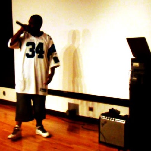
Darryl Dewayne Walker
age ~60
from Greensboro, NC
- Also known as:
-
- Darryl D Walker
- Darryl P Walker
- Darrell D Walker
- Darry L Walker
- Walker Walker
- Darryl Walkersr
- Phone and address:
- 1717 Fairfax Rd APT G, Greensboro, NC 27407
Darryl Walker Phones & Addresses
- 1717 Fairfax Rd APT G, Greensboro, NC 27407
- League City, TX
- Plano, TX
- Dallas, TX
- Lovettsville, VA
Work
-
Company:Maya 7
-
Specialities:graphic design
Education
-
School / High School:ComputER, Florida State UniversityApr 2007
Us Patents
-
Substrate Slew Circuit
view source -
US Patent:52668436, Nov 30, 1993
-
Filed:Mar 16, 1993
-
Appl. No.:8/032740
-
Inventors:Darryl Walker - Dallas TX
Daniel F. McLaughlin - Dallas TX -
Assignee:Texas Instruments Incorporated - Dallas TX
-
International Classification:H03K 301
H03K 17687 -
US Classification:3072962
-
Abstract:The described embodiments of the present invention provide a substrate slew circuit that eliminates electron injection. The slew circuit comprises a semiconductor substrate, at least one transistor and a control circuit. One of a source/drain of a first transistor in the slew circuit is connected to Vss, the other of the source/drain of the first transistor is connected to the gate and one of a source/drain of a second transistor, the other of the source/drain of the second transistor is connected to the substrate. A control circuit is connected to the gate of the first transistor for controlling the passage of voltage from the one of a source/drain of the first transistor to the substrate via the gate and the one of a source/drain of the second transistor. The sensitivity of the slew circuit can be made programmable by adding one or more more n-channel transistors in stacked diode configuration between the other of the source/drain of the first transistor and the substrate.
-
Block Specific Spare Circuit
view source -
US Patent:55766331, Nov 19, 1996
-
Filed:Jun 7, 1995
-
Appl. No.:8/484224
-
Inventors:Robert N. Rountree - Plano TX
Dan Cline - Plano TX
Darryl G. Walker - Sugar Land TX
Francis Hii - Singapore, SG
David W. Bergman - Bedford TX -
Assignee:Texas Instruments Incorporated - Dallas TX
-
International Classification:H03K 19003
G06F 1116 -
US Classification:326 10
-
Abstract:A circuit for selecting a block spare in a semiconductor device is designed with a programmable circuit (14), storing an internal address and producing an address match signal AM and a block select signal BS in response to first (A) and second (B) address signals and the internal address. A global spare circuit (28) produces a global spare select signal (GSS), in response to the address match signal. A block spare circuit (34) produces a block spare select signal (BSS), in response to the global spare select signal and the block select signal.
-
Apparatus And Method For An Active Field Plate Bias Generator
view source -
US Patent:55089623, Apr 16, 1996
-
Filed:Jun 29, 1994
-
Appl. No.:8/267701
-
Inventors:Daniel F. McLaughlin - Dallas TX
Darryl G. Walker - Sugar Land TX -
Assignee:Texas Instruments Incorporated - Dallas TX
-
International Classification:G11C 1124
-
US Classification:36518909
-
Abstract:The plate voltage for a Dynamic Random Access Memory storage cell array is provided by two amplifiers. The first amplifier operates at a relatively low power level and compensates for leakage in the storage cell array, the compensation initiated by a departure of the plate from a nominal value which exceeds a preselected amount. The second amplifier operates at a higher power level and provides compensation for transients in the plate voltage resulting from the charging and discharging of the storage cells. Because the transients occur when the storage cells are accessed, the second amplifier is enabled only when a group of storage cells is accessed. In addition to operating at a higher power level, the second amplifier is more sensitive and responds to smaller excursions from the nominal voltage. Both the first and the second amplifiers have separate driver circuits for responding to excursions above and for responding to excursions below the nominal voltage.
-
Substrate Slew Circuit Process
view source -
US Patent:53427998, Aug 30, 1994
-
Filed:Feb 22, 1993
-
Appl. No.:8/020486
-
Inventors:Darryl Walker - Dallas TX
Daniel F. McLaughlin - Dallas TX -
Assignee:Texas Instruments Incorporated - Dallas TX
-
International Classification:H01L 21335
-
US Classification:437 51
-
Abstract:The described embodiments of the present invention provide a substrate slew circuit that eliminates electron injection. The slew circuit comprises a semiconductor substrate, at least one transistor and a control circuit. One of source/drain of a first transistor (26) in the slew circuit is connected to Vss, the other of the source/drain of the first transistor (26) is connected to the substrate, or in another embodiment of the invention, to one of a source/drain of a second transistor (28), the gate and other of the source/drain of the second transistor (28) being connected to the substrate. A control circuit is connected to the gate of the first transistor for controlling the passage of voltage from the one of a source/drain of the first transistor (26) to the substrate via the gate and the one of a source/drain of the second transistor (28). The sensitivity of the slew circuit can be made programmable by adding p-channel transistors in stacked diode configuration between the other of the source/drain of the first transistor (26) and the substrate.
-
Substrate Slew Circuit Providing Reduced Electron Injection
view source -
US Patent:53131118, May 17, 1994
-
Filed:Aug 11, 1993
-
Appl. No.:8/105487
-
Inventors:Darryl Walker - Dallas TX
Daniel F. McLaughlin - Dallas TX -
Assignee:Texas Instruments Incorporated - Dallas TX
-
International Classification:H03K 301
-
US Classification:3072962
-
Abstract:The described embodiments of the present invention provide a substrate slew circuit that eliminates electron injection. The slew circuit comprises a semiconductor substrate, first and second transistors and a control circuit. One of a source/drain of the source/drain of the first transistor is connected to a reference voltage. One of a source/drain of the second transistor is connected to a gate of the first transistor, the other of the source/drain of the second transistor is coupled to receive a first voltage signal from a substrate pump. The control circuit is connected to the gate of the second transistor for controlling the passage of current from the other of the source/drain of the second transistor to the one of a source/drain of the second transistor.
-
Block Specific Spare Circuit
view source -
US Patent:55482252, Aug 20, 1996
-
Filed:May 26, 1994
-
Appl. No.:8/249499
-
Inventors:Robert N. Rountree - Plano TX
Dan Cline - Plano TX
Darryl G. Walker - Sugar Land TX
Francis Hii - Toa Payoh, SG
David W. Bergman - Bedford TX -
Assignee:Texas Instruments Incorportated - Dallas TX
-
International Classification:H03K 19003
-
US Classification:326 13
-
Abstract:A circuit for selecting a block spare in a semiconductor device is designed with a programmable circuit (14), storing an internal address and producing an address match signal AM and a block select signal BS in response to first (A) and second (B) address signals and the internal address. A global spare circuit (28) produces a global spare select signal (GSS), in response to the address match signal. A block spare circuit (34) produces a block spare select signal (BSS), in response to the global spare select signal and the block select signal.
Name / Title
Company / Classification
Phones & Addresses
PAID IN FULL MINISTRIES, INC
Resumes

Darryl Walker
view source
Darryl Walker
view source
Darryl Walker
view source
Darryl Walker
view source
Darryl Walker
view source
Darryl Walker
view sourceLocation:
United States

Darryl Walker
view sourceLocation:
United States

Darryl E . Walker
view sourceLawyers & Attorneys

Darryl Walker - Lawyer
view sourceISLN:
922620608
Admitted:
2000
University:
Santa Clara Univ SOL, Santa Clara, CA; Oklahoma St Univ, Stillwater, OK
Classmates

Darryl Walker
view sourceSchools:
Parkway Program High School Philadelphia PA 1995-1999
Community:
Rachel Pio, Stephanie Mathis, Willie Murdock, Scot Briggs

Darryl Walker
view sourceSchools:
Hampton Elementary School Hampton GA 1994-1998
Community:
Eydie Pease, Kim Adams, Shannon Swanson

Darryl Walker
view sourceSchools:
Our Lady of Lourdes School Philadelphia PA 1975-1983
Community:
Irene Caldi, Francis Lawless, John Bradley, Robert Bauersmith

Darryl Walker
view sourceSchools:
Gesu School Philadelphia PA 1995-1999
Community:
Gerson Sigman, Sandra Moore

Darryl Walker
view sourceSchools:
South High School Youngstown OH 1962-1966
Community:
Darell Willie, Angela Sanders, Ernest Anderson

Darryl Walker
view sourceSchools:
Hylton High School Woodbridge VA 2004-2008
Community:
Eric Baptist, Shawna Rogers, Anitra Harris

Darryl Walker
view sourceSchools:
Edmondson High School 400 Baltimore MD 2003-2007

Darryl Walker
view sourceSchools:
Cunard Junior High School Halifax Swaziland 1978-1982
Community:
Tanya Iceton
Youtube
Plaxo

Darryl Walker
view sourceNewmarket, NHLead Consultant at Synergy Resources, LLC Past: Professional Services Engineer at Infor Global Solutions, Professional Services Engineer...

Darryl Walker
view source
darryl Walker
view sourceJohnson and Johnson

Darryl E. Walker
view sourcePast: Dewberry

Le'Darryl Walker
view source
Darryl Walker Jr.
view source
Darryl Yogi Walker
view source
Darryl Walker Sr.
view source
Darryl SkateorDie Walker
view source
Darryl Walker Sr
view source
Darryl Walker Sr.
view source
Darryl J. Walker
view sourceMyspace
Googleplus

Darryl Walker
Work:
Synergy Resources, LLC - MFG Lead Consultant (2006)

Darryl Walker
About:
I punched a baby once. In my defense the baby was being kind of a dick.
Tagline:
I punched a baby once. In my defense the baby was being kind of a dick.
Bragging Rights:
Writer of the online web comic Press Start To Play.

Darryl Walker

Darryl Walker

Darryl Walker

Darryl Walker

Darryl Walker

Darryl Walker
Get Report for Darryl Dewayne Walker from Greensboro, NC, age ~60


