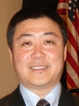
Hong Shen
age ~48
from Foothill Ranch, CA
Hong Shen Phones & Addresses
- 28 Verona Ln, Foothill Rnch, CA 92610
- Foothill Ranch, CA
- 20 Palatine APT 414, Irvine, CA 92612
- Thousand Oaks, CA
- Winnetka, CA
- Fort Collins, CO
- Winnetka, CA
- Ventura, CA
- Foothill Rnch, CA
Lawyers & Attorneys

Hong Shen, Westlake Village CA - Lawyer
view sourceAddress:
5707 Corsa Ave. Suit 106, Westlake Village, CA 91362
8054914005 (Office)
8054914005 (Office)
Licenses:
California - Active 2010
Experience:
Attorney at Roberts Law Group - 2010-present
Education:
Concord Law School
Specialties:
Business - 50%, years, 8 cases
Patent Application - 25%, years, 6 cases
Trademark Application - 25%, years, 8 cases
Patent Application - 25%, years, 6 cases
Trademark Application - 25%, years, 8 cases
Languages:
English
Mandarin
Mandarin
Associations:
American Bar Association
Description:
Patent attorney at your service
I have a PhD in chemistry and have been working in semiconductor industry for years. I am licensed in California and also...

Hong Shen - Lawyer
view sourceSpecialties:
Business
Patent Application
Trademark Application
Patent Application
Patent Application
Trademark Application
Patent Application
ISLN:
922528828
Admitted:
2010
University:
Concord Law School; Los Angeles CA; Foreign School

Hong Shen - Lawyer
Us Patents
-
Gaas Integrated Circuit Device And Method Of Attaching Same
view source -
US Patent:7923842, Apr 12, 2011
-
Filed:Mar 16, 2006
-
Appl. No.:11/377690
-
Inventors:Hong Shen - Camarillo CA, US
Ravi Ramanathan - Thousand Oaks CA, US
Qiuliang Luo - Moorpark CA, US
Robert W Warren - Newport Beach CA, US
Usama K Abdali - Aliso Viejo CA, US -
Assignee:Skyworks Solutions, Inc. - Woburn MA
-
International Classification:H01L 23/48
-
US Classification:257774, 257E23011, 257E23067
-
Abstract:A gallium arsenide (GaAs) integrated circuit device is provided. The GaAs circuit device has a GaAs substrate with a copper contact layer for making electrical ground contact with a pad of a target device. Although copper is known to detrimentally affect GaAS devices, the copper contact layer is isolated from the GaAs substrate using a barrier layer. The barrier layer may be, for example, a layer of nickel vanadium (NiV). This nickel vanadium (NiV) barrier protects the gallium arsenide substrate from the diffusion effects of the copper contact layer. An organic solder preservative may coat the exposed copper to reduce oxidation effects. In some cases, a gold or copper seed layer may be deposited on the GaAs substrate prior to depositing the copper contact layer.
-
Etched Wafers And Methods Of Forming The Same
view source -
US Patent:8415805, Apr 9, 2013
-
Filed:Dec 17, 2010
-
Appl. No.:12/971465
-
Inventors:Hong Shen - Camarillo CA, US
-
Assignee:Skyworks Solutions, Inc. - Woburn MA
-
International Classification:H01L 23/48
-
US Classification:257774, 257E21023, 257E21231, 438717
-
Abstract:Etched wafers and methods of forming the same are disclosed. In one embodiment, a method of etching a wafer is provided. The method includes forming a metal hard mask on the wafer using electroless plating, patterning the metal hard mask, and etching a plurality of features on the wafer using an etcher. The plurality of featured are defined by the metal hard mask.
-
Gaas Integrated Circuit Device And Method Of Attaching Same
view source -
US Patent:20110186966, Aug 4, 2011
-
Filed:Apr 11, 2011
-
Appl. No.:13/084467
-
Inventors:Hong Shen - Camarillo CA, US
Ravi Ramanathan - Thousand Oaks CA, US
Qiuliang Luo - Moorpark CA, US
Robert W. Warren - Newport Beach CA, US
Usama K. Abdali - Aliso Viejo CA, US -
Assignee:SKYWORKS SOLUTIONS, INC. - Woburn MA
-
International Classification:H01L 29/20
H01L 21/283 -
US Classification:257615, 438653, 257E29089, 257E21159
-
Abstract:A gallium arsenide (GaAs) integrated circuit device is provided. The GaAs circuit device has a GaAs substrate with a copper contact layer for making electrical ground contact with a pad of a target device. Although copper is known to detrimentally affect GaAs devices, the copper contact layer is isolated from the GaAs substrate using a barrier layer. The barrier layer may be, for example, a layer of nickel vanadium (NiV). This nickel vanadium (NiV) barrier protects the gallium arsenide substrate from the diffusion effects of the copper contact layer. An organic solder preservative may coat the exposed copper to reduce oxidation effects. In some cases, a gold or copper seed layer may be deposited on the GaAs substrate prior to depositing the copper contact layer.
-
Methods For Metal Plating And Related Devices
view source -
US Patent:20120153477, Jun 21, 2012
-
Filed:Dec 17, 2010
-
Appl. No.:12/972119
-
Inventors:Hong Shen - Westlake Village CA, US
-
Assignee:SKYWORKS SOLUTIONS, INC. - Woburn MA
-
International Classification:H01L 23/532
H01L 21/768 -
US Classification:257751, 438606, 257E21584, 257E23155
-
Abstract:Methods for plating metal over features of a semiconductor wafer and devices that can be formed by these methods are disclosed. One such method includes forming a barrier layer over the substrate using electroless plating and forming a copper layer over the barrier layer. In some implementations, the semiconductor wafer is a GaAs wafer. Alternatively or additionally, the feature over which metal is plated can be a through-wafer via. In some implementations, a seed layer over the barrier layer can be formed using electroless plating.
-
Methods Of Stress Balancing In Gallium Arsenide Wafer Processing
view source -
US Patent:20130193573, Aug 1, 2013
-
Filed:Jan 27, 2012
-
Appl. No.:13/360489
-
Inventors:Hong Shen - Oak Park CA, US
-
Assignee:SKYWORKS SOLUTIONS, INC. - Woburn MA
-
International Classification:H01L 23/48
H01L 21/28
H01L 21/66 -
US Classification:257741, 438 14, 438597, 438686, 257E21521, 257E2301, 257E21158
-
Abstract:Systems, apparatuses, and methods related to the design, fabrication, and manufacture of gallium arsenide (GaAs) integrated circuits are disclosed. Copper can be used as the contact material for a GaAs integrated circuit. Metallization of the wafer and through-wafer vias can be achieved through copper plating processes disclosed herein. To avoid warpage, the tensile stress of a conductive layer deposited onto a GaAs substrate can be offset by depositing a compensating layer having negative stress over the GaAs substrate. GaAs integrated circuits can be singulated, packaged, and incorporated into various electronic devices.
-
Optimization Of Copper Plating Through Wafer Via
view source -
US Patent:20130193575, Aug 1, 2013
-
Filed:Jan 27, 2012
-
Appl. No.:13/360431
-
Inventors:Hong Shen - Oak Park CA, US
-
Assignee:SKYWORKS SOLUTIONS, INC. - Woburn MA
-
International Classification:H01L 23/48
H01L 21/768
H01L 21/02 -
US Classification:257751, 438758, 257741, 438667, 257E21002, 257E2301, 257E21586, 257E23011
-
Abstract:Systems, apparatuses, and methods related to the design, fabrication, and manufacture of gallium arsenide (GaAs) integrated circuits are disclosed. Copper can be used as the contact material for a GaAs integrated circuit. Metallization of the wafer and through-wafer vias can be achieved through copper plating processes disclosed herein. To improve the copper plating, a seed layer formed in the through-wafer vias can be modified to increase water affinity, rinsed to remove contaminants, and activated to facilitate copper deposition. GaAs integrated circuits can be singulated, packaged, and incorporated into various electronic devices.
-
Gallium Arsenide Devices With Copper Backside For Direct Die Solder Attach
view source -
US Patent:20130249095, Sep 26, 2013
-
Filed:Mar 26, 2012
-
Appl. No.:13/429725
-
Inventors:Hong Shen - Oak Park CA, US
-
Assignee:SKYWORKS SOLUTIONS, INC. - Woburn MA
-
International Classification:H01L 23/48
H01L 21/50 -
US Classification:257751, 438121, 257E2301, 257E21499
-
Abstract:Systems, apparatuses, and methods related to the design, fabrication, and manufacture of gallium arsenide (GaAs) integrated circuits are disclosed. Copper can be used as the contact material for a GaAs integrated circuit. Metallization of the wafer and through-wafer vias can be achieved through copper plating processes disclosed herein. Direct die solder (DDS) attach can be achieved by use of electroless nickel plating of the copper contact layer followed by a palladium flash. GaAs integrated circuits can be singulated, packaged, and incorporated into various electronic devices.
-
Process For Fabricating Gallium Arsenide Devices With Copper Contact Layer
view source -
US Patent:20130299985, Nov 14, 2013
-
Filed:May 8, 2012
-
Appl. No.:13/466792
-
Inventors:Hong Shen - Oak Park CA, US
-
Assignee:SKYWORKS SOLUTIONS, INC. - Woburn MA
-
International Classification:H01L 23/532
H01L 21/283 -
US Classification:257741, 438687, 257E23155, 257E21159
-
Abstract:Systems, apparatuses, and methods related to the design, fabrication, and manufacture of gallium arsenide (GaAs) integrated circuits are disclosed. Copper can be used as the contact material for a GaAs integrated circuit. Metallization of the wafer and through-wafer vias can be achieved through copper plating processes disclosed herein. Various protocols can be employed during processing to avoid cross-contamination between copper-plated and non-copper-plated wafers. GaAs integrated circuits can be singulated, packaged, and incorporated into various electronic devices.
Name / Title
Company / Classification
Phones & Addresses
Director, President, Secretary, Treasurer
Sh Southpoint Corp
Director of Engineering
Skyworks Solutions, Inc
Mfg Semiconductors/Related Devices · Electrician · Electrical Contrs
Mfg Semiconductors/Related Devices · Electrician · Electrical Contrs
2427 W Hillcrest Dr, Thousand Oaks, CA 91320
2421 W Hillcrest Dr, Newbury Park, CA 91320
8054804385, 8054804100
2421 W Hillcrest Dr, Newbury Park, CA 91320
8054804385, 8054804100
Resumes

Health, Wellness And Fitness Professional
view sourceLocation:
Orange County, California Area

Hong Shen
view sourceLocation:
United States

Hong Shen
view sourceLocation:
United States

Attorney
view sourcePosition:
Attorney at law at Roberts Law Group
Location:
Greater Los Angeles Area
Industry:
Legal Services
Work:
Roberts Law Group since Jun 2010
Attorney at law
Attorney at law
Education:
Concord Law School - Kaplan University
zeying ma
zeying ma

Hong Shen
view sourceLocation:
United States

Hong Shen
view sourceLocation:
United States

Hong Shen
view sourceLocation:
United States
Medicine Doctors

Hong Shen
view sourceSpecialties:
Family Medicine
Work:
Shen Medical Associates
3100 4 St, Longview, TX 75605
9032474404 (phone), 9032474408 (fax)
3100 4 St, Longview, TX 75605
9032474404 (phone), 9032474408 (fax)
Education:
Medical School
University of Texas Medical School at San Antonio
Graduated: 1998
University of Texas Medical School at San Antonio
Graduated: 1998
Procedures:
Cardiac Stress Test
Arthrocentesis
Destruction of Benign/Premalignant Skin Lesions
Electrocardiogram (EKG or ECG)
Skin Tags Removal
Vaccine Administration
Arthrocentesis
Destruction of Benign/Premalignant Skin Lesions
Electrocardiogram (EKG or ECG)
Skin Tags Removal
Vaccine Administration
Conditions:
Dementia
Osteoarthritis
Pneumonia
Abnormal Vaginal Bleeding
Acne
Osteoarthritis
Pneumonia
Abnormal Vaginal Bleeding
Acne
Languages:
Chinese
English
Spanish
English
Spanish
Description:
Dr. Shen graduated from the University of Texas Medical School at San Antonio in 1998. He works in Longview, TX and specializes in Family Medicine. Dr. Shen is affiliated with Good Shepherd Medical Center and Longview Regional Medical Center.

Hong Shen
view sourceSpecialties:
Gastroenterology
Work:
The Oregon ClinicThe Oregon Clinic Gastroenterology - East At Gateway
1111 NE 99 Ave STE 301, Portland, OR 97220
5039632707 (phone), 5039632802 (fax)
Oregon ClinicOregon Clinic Gastroenterology East
10330 SE 32 Ave STE 210, Portland, OR 97222
5039632707 (phone), 5039632802 (fax)
1111 NE 99 Ave STE 301, Portland, OR 97220
5039632707 (phone), 5039632802 (fax)
Oregon ClinicOregon Clinic Gastroenterology East
10330 SE 32 Ave STE 210, Portland, OR 97222
5039632707 (phone), 5039632802 (fax)
Education:
Medical School
Univ of Western Australia, Fac of Med & Dent, Perth, Wa, Australia
Graduated: 1997
Univ of Western Australia, Fac of Med & Dent, Perth, Wa, Australia
Graduated: 1997
Procedures:
Colonoscopy
Sigmoidoscopy
Upper Gastrointestinal Endoscopy
Vaccine Administration
Sigmoidoscopy
Upper Gastrointestinal Endoscopy
Vaccine Administration
Conditions:
Abdominal Hernia
Acute Pancreatitis
Acute Pharyngitis
Anal Fissure
Anemia
Acute Pancreatitis
Acute Pharyngitis
Anal Fissure
Anemia
Languages:
English
Description:
Dr. Shen graduated from the University of Western Australia in Perth. He later completed his internship and residency at Fremantle Hospital in Fremantle, Australia. Dr. Shen finished his internal medicine residency and gastroenterology fellowship at Indiana University Medical Center. He has been awarded the Travel Award for managing a Hepatitis B workshop and was the Acting Chief for the

Hong H. Shen
view sourceSpecialties:
Pain Management
Work:
Cleveland ClinicLutheran Hospital Pain Management Center
1730 W 25 St STE 4A, Cleveland, OH 44113
2163632391 (phone), 2163632107 (fax)
1730 W 25 St STE 4A, Cleveland, OH 44113
2163632391 (phone), 2163632107 (fax)
Education:
Medical School
Suzhou Med Coll, Suzhou City, Jiangsu, China
Graduated: 1984
Suzhou Med Coll, Suzhou City, Jiangsu, China
Graduated: 1984
Procedures:
Neurological Testing
Physical Therapy
Physical Therapy Evaluation
Physical Therapy
Physical Therapy Evaluation
Languages:
English
Spanish
Spanish
Description:
Dr. Shen graduated from the Suzhou Med Coll, Suzhou City, Jiangsu, China in 1984. She works in Cleveland, OH and specializes in Pain Management. Dr. Shen is affiliated with Cleveland Clinic and Lutheran Hospital.

Hong Shen
view sourceIsbn (Books And Publications)

PDCAT 2005: 5-8 December 2005, Dalian, China Proceedings
view sourceAuthor
Hong Shen
ISBN #
0769524052

Parallel and Distributed Computing, Applications and Technologies: PDCAT'2003 Proceedings [August 27-29, 2003, Chengdu, China
view sourceAuthor
Hong Shen
ISBN #
0780378407


Parallel And Distributed Computing:Applications And Technologies: 5th International Conference, Pdcat 2004, Singapore, December 8-10, 2004, Proceedings
view sourceAuthor
Hong Shen
ISBN #
3540240136


1793:Ying Guo Shi Tuan Hua Jia Bi Xia De Qianlong Sheng Shi: Zhongguo Ren De Fu Shi He Xi Su Tu Jian
view sourceAuthor
Hong Shen
ISBN #
7807150777

Hong Shen
view source
Hong Shen
view source
Hong Shen
view source
Hong Shen
view source
Hong Shen
view source
Hong Janet Shen
view source
Hong Lit Shen
view source
Hong Ling Shen
view sourceYoutube
Plaxo

SHEN, Hong (Henry)
view sourceShanghai, ChinaGovernment Relations, China at The Dow Chemical Co...

hong shen
view sourceMTS ALLSTREAM

Hong Shen
view sourceSenior Manager at Flextronics
Classmates

Hong Shen
view sourceSchools:
Unversity of Ottawa Ottawa Morocco 2003-2007
Community:
Louis Souliere, James Carlin, Roberta Simpson

Hong Shen | Silverthorn C...
view source
Silverthorn Collegiate In...
view sourceGraduates:
Aida Fantilli (1978-1982),
Annette Pastorek (1980-1984),
Hong Shen (2003-2007),
Bob Smith (1975-1979),
Karen McIlheron (1984-1988)
Annette Pastorek (1980-1984),
Hong Shen (2003-2007),
Bob Smith (1975-1979),
Karen McIlheron (1984-1988)

Red Deer College, Red dee...
view sourceGraduates:
Hong Shen (2001-2005),
Mike Swaren (1996-1998),
Carmen Stephenson (2004-2004)
Mike Swaren (1996-1998),
Carmen Stephenson (2004-2004)
Myspace
Flickr
Googleplus

Hong Shen

Hong Shen
Relationship:
Married

Hong Shen

Hong Shen

Hong Shen

Hong Shen

Hong Shen

Hong Shen
Get Report for Hong Shen from Foothill Ranch, CA, age ~48


