James C Yu
age ~39
from Oakland, CA
James Yu Phones & Addresses
- Oakland, CA
- 16020 White Bird St, Beaverton, OR 97007 • 5035240573
Medicine Doctors

James B. Yu
view sourceSpecialties:
Radiation Oncology
Work:
Yale Medical GroupLawrence & Memorial Cancer Center
230 Pkwy S, Waterford, CT 06385
8604443744 (phone), 8602714210 (fax)
Yale Medical GroupYale Brain Tumor Center
35 Park St FL 8, New Haven, CT 06519
2037857284 (phone), 2037372591 (fax)
Yale University Radiology Oncology
333 Cedar St FL 1, New Haven, CT 06510
2037852956 (phone), 2037854622 (fax)
Yale Medical GroupYale Radiation Oncology
35 Park St, New Haven, CT 06519
2032002100 (phone), 2032002180 (fax)
Yale Medical GroupYale New Haven Hospital Radiation Oncology
20 York St, New Haven, CT 06510
2037855175 (phone), 2037854622 (fax)
Education:
Medical School
University of Michigan Medical School
Graduated: 2004
University of Michigan Medical School
Graduated: 2004
Languages:
English
Spanish
Spanish
Description:
Dr. Yu graduated from the University of Michigan Medical School in 2004. He works in New Haven, CT and 4 other locations and specializes in Radiation Oncology. Dr. Yu is affiliated with Bridgeport Hospital, Lawrence Memorial Hospital, William W Backus Hospital and Yale New Haven Hospital.

James Z. Yu
view sourceSpecialties:
Emergency Medicine
Work:
Tristar Greenview Regional Hospital Emergency
1801 Ashley Cir, Bowling Green, KY 42104
2707932150 (phone), 2707932055 (fax)
1801 Ashley Cir, Bowling Green, KY 42104
2707932150 (phone), 2707932055 (fax)
Languages:
English
Description:
Dr. Yu works in Bowling Green, KY and specializes in Emergency Medicine. Dr. Yu is affiliated with Tristar Greenview Regional Hospital.
Us Patents
-
Cross-Shaped Resist Dispensing System And Method
view source -
US Patent:6403500, Jun 11, 2002
-
Filed:Jan 12, 2001
-
Appl. No.:09/760241
-
Inventors:James Jiahua Yu - Milpitas CA
Kouros Ghandehari - Santa Clara CA
Bhanwar Singh - Morgan Hill CA -
Assignee:Advanced Micro Devices, Inc. - Sunnyvale CA
-
International Classification:H01L 2131
-
US Classification:438782, 438778, 438780, 427 96, 427240
-
Abstract:An exemplary method of depositing photoresist material on an integrated circuit wafer is described. This method can include providing a cross-shaped resist dispenser including a plurality of resist dispense nozzles; dispensing photoresist material through the plurality of resist dispense nozzles to an integrated circuit wafer; and rotating at least one of the cross-shaped resist dispenser and the integrated circuit wafer.
-
Method Of Using Controlled Resist Footing On Silicon Nitride Substrate For Smaller Spacing Of Integrated Circuit Device Features
view source -
US Patent:6514874, Feb 4, 2003
-
Filed:Jun 6, 2001
-
Appl. No.:09/875635
-
Inventors:James Jiahua Yu - Milpitas CA
Bhanwar Singh - Morgan Hill CA
Angela T. Hui - Fremont CA -
Assignee:Advanced Micro Devices, Inc. - Sunnyvale CA
-
International Classification:H01L 21461
-
US Classification:438744, 438672, 438735
-
Abstract:A method of fabricating an integrated circuit can include providing a layer of silicon nitride over a semiconductor substrate where the layer of silicon nitride has a first thickness selected based on a desired size of extensions; providing a layer of photoresist material over the layer of silicon nitride; patterning the layer of photoresist to form photoresist features being separated at the top of the photoresist features by one minimum lithographic feature and etching a portion of the layer of silicon nitride to form a hole for an integrated circuit device feature. The photoresist features include extensions at the bottom of the photoresist features. The extensions define footings. These footings reduce the separation at the bottom of the photoresist features. As such, exposed portions of the layer of silicon nitride are less than one minimum lithographic feature in width.
-
Digital Trust Center For Medical Image Authentication
view source -
US Patent:6557102, Apr 29, 2003
-
Filed:Sep 5, 1997
-
Appl. No.:08/924867
-
Inventors:Stephen T. Wong - San Francisco CA
James Yuan-Pin Yu - Sunnyvale CA -
Assignee:Koninklijke Philips Electronics N.V. - Eindhoven
-
International Classification:H04L 900
-
US Classification:713176, 705 3
-
Abstract:A medical image management system including an image archive server for storing image datasets received from a plurality of image acquisition computers and a plurality of display stations for displaying requested image datasets retrieved from the image archive server is provided with an authentication and security system which includes an authentication server for maintaining and storing hashes and timestamps, and for providing hash, timestamp pairs in encrypted form in response to requests from display stations. The image acquisition computers are configured for computing hashes and providing them and image dataset identifiers to the authentication server, receiving timestamps from the authentication server which are then inserted in the image datasets, and storing the image datasets in the image archive server. The display stations are configured for retrieving image dataset, computing hashes from retrieved image datasets, requesting and decrypting hash/timestamp pairs received from the authentication server, and comparing the hashes, and optionally the timestamps, obtained from the authentication server with those computed or extracted from the image datasets received from the image archive server.
-
System For And Method Of Using Developer As A Solvent To Spread Photoresist Faster And Reduce Photoresist Consumption
view source -
US Patent:6592939, Jul 15, 2003
-
Filed:Jun 6, 2001
-
Appl. No.:09/875596
-
Inventors:James Jiahua Yu - Milpitas CA
-
Assignee:Advanced Micro Devices, Inc. - Sunnyvale CA
-
International Classification:B05D 312
-
US Classification:427240, 427402, 4274071, 427425, 118 52, 118320, 438758
-
Abstract:An exemplary method of using developer as a solvent to spread photoresist faster and reduce photoresist consumption can include dispensing a developer solution onto an integrated circuit wafer, spinning the integrated circuit wafer to distribute the developer solution over the integrated circuit wafer, and dispensing a photoresist solution onto the integrated circuit covered with the developer solution.
-
Digital Phase Locked Loops For Packet Stream Rate Matching And Restamping
view source -
US Patent:7333468, Feb 19, 2008
-
Filed:May 16, 2005
-
Appl. No.:11/129798
-
Inventors:Sebastian Turullols - Los Altos CA, US
Aly E. Orady - Sunnyvale CA, US
James J. Yu - San Jose CA, US
Andrew C. Yang - Sunnyvale CA, US -
Assignee:Sun Microsystems, Inc. - Santa Clara CA
-
International Classification:H04J 3/24
H04J 3/06
H04L 12/56
H04L 7/00
H04L 7/04
H04L 9/00
H04B 1/18
H04B 1/10 -
US Classification:370349, 370350, 37039562, 370509, 370514, 4551803, 4551811, 4551832, 375357, 375366, 375362, 375350, 375355, 713178
-
Abstract:A packet stream multiplexer may include one or more control loops (e. g. , digital phase locked loops) for tracking the source clock frequency associated with a packet stream. A first control loop may slowly drive an error between a received timestamp and an estimated timestamp to zero. A second control loop may more quickly drive a first derivative of the error to zero. The second control loop may include a set of digital filters ordered according to tracking speed. The output of the slowest filter is initially selected for updating the source clock frequency estimate. As time progresses, the faster filters are selected in succession. The estimated source clock frequency is used to restamp packets of the packet stream as they are sent out onto an output channel.
-
Shared Virtual Network Interface
view source -
US Patent:7912082, Mar 22, 2011
-
Filed:Jun 9, 2008
-
Appl. No.:12/135348
-
Inventors:Andrew C. Yang - Sunnyvale CA, US
James J. Yu - San Jose CA, US -
Assignee:Oracle America, Inc. - Redwood City CA
-
International Classification:H04L 12/66
-
US Classification:370463
-
Abstract:A system includes one or more processing units coupled to a network interface unit. The network interface unit may include a network port for connection to a network and a virtual interface that may be configured to distribute an available communication bandwidth of the network port between the one or more processing units. The network port may include a shared media access control (MAC) unit. The virtual interface may include a plurality of processing unit resources each associated with a respective one of the one or more processing units. Each of the processing unit resources may include an I/O interface unit coupled to a respective one of the one or more processing units via an I/O interconnect, and an independent programmable virtual MAC unit that is programmably configured by the respective one of the one or more processing units. The virtual interface may also include a receive datapath and a transmit datapath that are coupled between and shared by the plurality of processing unit resources and the network port.
-
Capacitor Coupled Ethernet
view source -
US Patent:8044747, Oct 25, 2011
-
Filed:Apr 30, 2009
-
Appl. No.:12/433080
-
Inventors:James Yu - San Francisco CA, US
Minh Tran - San Jose CA, US -
Assignee:Broadcom Corporation - Irvine CA
-
International Classification:H03H 2/00
H04B 3/00 -
US Classification:333 24R, 375257
-
Abstract:A system and method for enabling power applications over a single conductor pair. In one embodiment, data transformers are coupled to a single conductor pair using one or more direct current (DC) blocking elements that preserve an alternating current path. Power is injected onto the single conductor pair after the DC blocking elements and power is extracted from the single conductor pair before the DC blocking elements. Saturation of the data transformers by the injection of power onto the single pair is thereby prevented.
-
Active Powered Device For The Application Of Power Over Ethernet
view source -
US Patent:20090222678, Sep 3, 2009
-
Filed:Feb 29, 2008
-
Appl. No.:12/040593
-
Inventors:James Yu - San Francisco CA, US
Minh Tran - San Jose CA, US -
Assignee:Broadcom Corporation - Irvine CA
-
International Classification:G06F 1/26
-
US Classification:713300
-
Abstract:An active powered device (PD) for the application of power over Ethernet (PoE). In a fixed power budget environment, it is important for the power sourcing equipment (PSE) to accurately determine a power budget for the various powered ports. An active PD can be designed to gather additional information (e.g., current and input voltage) during PD operation and to forward the additional information to the PSE. The PSE can then use the additional information to adjust operational parameters such as a power budget.
Name / Title
Company / Classification
Phones & Addresses
CPA
Innovative Bancorp
State Commercial Banks
State Commercial Banks
360 14Th St, Oakland, CA 94612
President
Net Usa, Inc
Hardware Stores
Hardware Stores
103 Hammond Ave., Fremont, CA 94539
Vice President Marketing And Business Development
Applied Identity, Inc.
Security Systems Services
Security Systems Services
456 Montgomery St Ste 400, San Francisco, CA 94104
Senior Vice President, Marketing and Business Development
NeoScale Systems , Inc.
Motor Vehicle Dealers (New and Used)
Motor Vehicle Dealers (New and Used)
1655 Mccarthy Blvd., Milpitas, CA 95035
President
Eon Silicon Devices Inc
General Contractors-Single-Family Houses
General Contractors-Single-Family Houses
4655 Old Ironsides Dr # 480, Santa Clara, CA 95054
Website: eonsdi.com
Website: eonsdi.com
President
Eon Silicon Devices
Architect
Architect
4655 Old Ironsides Dr STE 480, Santa Clara, CA 95054
4082358680, 4082358685
4082358680, 4082358685
President
C.& J. Y. GROUP, INC
Nonclassifiable Establishments
Nonclassifiable Establishments
995 Montague Expwy #216, Milpitas, CA 95035
995 Montague Expy, Milpitas, CA 95035
995 Montague Expy, Milpitas, CA 95035
President
JAMES YU, DDS, INC
995 Montague Expy STE 216, Milpitas, CA 95035
Resumes

James Yu San Francisco, CA
view sourceWork:
Ziff Davis
Apr 2013 to 2000
LQT Analyst Anchor
San Francisco, CA
2012 to 2013
Sales Associate
Apr 2013 to 2000
LQT Analyst Anchor
San Francisco, CA
2012 to 2013
Sales Associate
Education:
University of California Davis
Davis, CA
2008 to 2011
B.A. in Psychology
Davis, CA
2008 to 2011
B.A. in Psychology
License Records
James Yu
License #:
E065584 - Expired
Category:
Emergency medical services
Issued Date:
Apr 3, 2009
Expiration Date:
Mar 31, 2011
Type:
Orange County EMS Agency
James Yu
License #:
E117760 - Active
Category:
Emergency medical services
Issued Date:
Feb 11, 2015
Expiration Date:
Nov 30, 2017
Type:
Riverside County EMS Agency
Isbn (Books And Publications)

Lawyers & Attorneys

James Yu - Lawyer
view sourceSpecialties:
Class Action
Commercial Litigation
Business Torts
Contract Disputes
Franchise, Dealer & Distributor Disputes
Product Liability
Trade Secrets, Computer Fraud & Non-Competes
Employment Litigation
Wage & Hour Litigation
Commercial Litigation
Business Torts
Contract Disputes
Franchise, Dealer & Distributor Disputes
Product Liability
Trade Secrets, Computer Fraud & Non-Competes
Employment Litigation
Wage & Hour Litigation
ISLN:
916067180
Admitted:
2000
University:
Johns Hopkins University, B.A., 1995
Law School:
Rutgers University Law School - Newark, J.D., 2000

James Yu - Lawyer
view sourceSpecialties:
Taxation
ISLN:
910065953
Admitted:
1995
University:
Dartmouth College, A.B., 1990
Law School:
New York University, LL.M., 1995; Vanderbilt University, J.D., 1994
Googleplus

James Yu
Lived:
Monterey Park, CA
Alhambra, CA
San Mateo, CA
Oakland, CA
Santa Clara, CA
Alhambra, CA
San Mateo, CA
Oakland, CA
Santa Clara, CA
Work:
AccelOps Inc. - Sr. Technical Support Engineer (2012)
ArcSight - Technical Support Engineer (2011-2012)
Barracuda Networks - Tier 2 Technical Support Engineer (2008-2011)
ArcSight - Technical Support Engineer (2011-2012)
Barracuda Networks - Tier 2 Technical Support Engineer (2008-2011)
Education:
California State University, Los Angeles - CIS
Relationship:
In_a_relationship
About:
Nom Nom Nom
Bragging Rights:
Still finding out about this google+ thing.
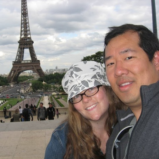
James Yu
Lived:
North Carolina
Texas
San Mateo, CA
San Antonio, TX
Austin, TX
Kansas City, KS
Texas
San Mateo, CA
San Antonio, TX
Austin, TX
Kansas City, KS
Education:
UT, UNC
Tagline:
Live life in constant, total amazement
Bragging Rights:
Successfully exported all my Facebook photos

James Yu
Lived:
Portland, OR
Work:
The Oregonian - Digital desk
The Oregonian
The Oregonian
Education:
University of Oregon - None

James Yu
Lived:
Sunnyvale, CA
Work:
Samsung research america
Education:
Anhui University
About:
Christian, Reformed
Tagline:
基督徒已婚两娃; Christian, married, two kids...

James Yu
Education:
Orange Coast College - Accounting & IT, UC Berkeley - Applied Math, Ohlone College - Math, John F. Kennedy High School

James Yu
Work:
Li Yu & Associates Ltd. - Director (2010)
Education:
Chu Hai College of Higher Education - Civil Engineering
About:
I am an expertise on design and build in small houses industry in Hong Kong.
Tagline:
My job is now major on design and build in small houses industry in Hong Kong. You are welcome to contact me if you need assistance in your small house development projects.
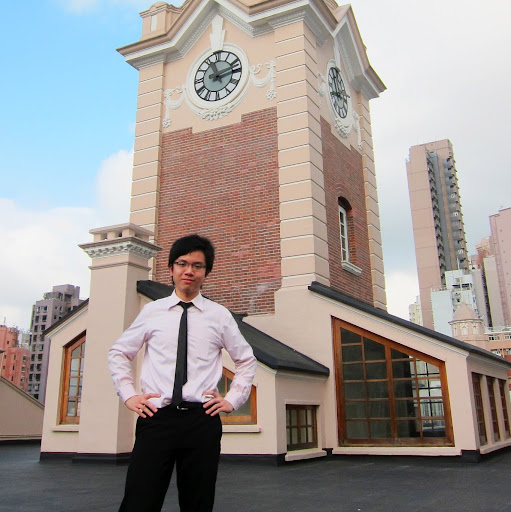
James Yu
Work:
HSBC - Summer internship (2011-2011)
Education:
The University of Hong Kong - Computer Science, Kiangsu-Chekiang College

James Yu
Tagline:
I'm James.
Youtube
Myspace
Plaxo

James Yu
view sourceFullerton, CAPastor at EFC Irvine

james yu
view sourceC.C.

James YU
view source
James Yu
view sourceMihaud International Co

James Yu
view sourceUnited States of America

James William Yu
view source
Michael James Yu
view source
James Christian Yu
view source
James Vincent Yu
view source
James Anthony Yu
view source
Ryan James Yu Zamora
view source
Rald James Yu Morales
view source
Patrick James Yu
view sourceClassmates

James Yu
view sourceSchools:
Vines High School Plano TX 1993-1997
Community:
Jimmie Eldridge, Donovan Clifton

James Yu
view sourceSchools:
Good Counsel High School Wheaton MD 1966-1970

James Yu
view sourceSchools:
Glenbard South High School Glen Ellyn IL 1986-1990

James Yu
view sourceSchools:
Alberta College Edmonton Azores 1970-1974
Community:
Marion Henry, Kurt Schacker, Ted Cutlan

James Yu
view sourceSchools:
Rundle College Calgary Azores 1987-1991
Community:
Jenni Bruce, Craig Chandler, Anjali Deshpande, Jay Regner, Mikel Bakalar

James Yu
view sourceSchools:
A.B. Newell Elementary School Grand Island NE 1997-2001
Community:
Jennifer Beck, Danielle Penner, Mallory Corbett, Alison Wit, Tiffany Gregory, Jacob Lawver, Chris Schwieger, Eric Carraher, Taylor Fredrickson, Susan Trimble

University of Alberta - B...
view sourceGraduates:
James Yu (1972-1976),
Michael Anderson (1985-1988),
Joni Petruskevich (1987-1991),
Ravi Bakshi (1979-1985)
Michael Anderson (1985-1988),
Joni Petruskevich (1987-1991),
Ravi Bakshi (1979-1985)

Vines High School, Plano,...
view sourceGraduates:
Christopher Cox (1987-1991),
Chrissy Johnson (1982-1984),
Lee Megason (1976-1978),
Bob Uruncle (1995-2000),
James Yu (1993-1997),
Michael Wissman (1983-1987)
Chrissy Johnson (1982-1984),
Lee Megason (1976-1978),
Bob Uruncle (1995-2000),
James Yu (1993-1997),
Michael Wissman (1983-1987)
Get Report for James C Yu from Oakland, CA, age ~39


