Jay L Goldman
age ~71
from Mountain View, CA
Jay Goldman Phones & Addresses
- 1411 Village Ct, Mountain View, CA 94040 • 6178035763
- Brewster, MA
- Medford, MA
- Palo Alto, CA
- Mansfield, MA
- Sharon, MA
Work
-
Company:Kaiser Permanente Medical Ctr
-
Address:27400 Hesperian Blvd, Hayward, CA 94545
-
Phones:5107844000
Education
-
School / High School:University Of Michigan Medical School1981
Languages
English • Chinese • Spanish • Vietnamese
Awards
Healthgrades Honor Roll
Ranks
-
Certificate:Emergency Medicine, 1999
Specialities
Internal Medicine • Emergency Medicine
Lawyers & Attorneys

Jay W. Goldman, Newton MA - Lawyer
view sourceAddress:
41 Vineyard Rd, Newton, MA 02459
6173086741 (Office)
6173086741 (Office)
Licenses:
Massachusetts - Active 1970

Jay Michael Goldman, San Francisco CA - Lawyer
view sourceAddress:
Office of the Attorney General
455 Golden Gate Ave Ste 11000, San Francisco, CA 94102
4157035846 (Office)
455 Golden Gate Ave Ste 11000, San Francisco, CA 94102
4157035846 (Office)
Licenses:
California - Active 1993
Education:
University of California, Hastings College of the Law
San Francisco State University
San Francisco State University

Jay Richard Goldman - Lawyer
view sourceLicenses:
Virginia - Authorized to practice law 1980

Jay Goldman - Lawyer
view sourceSpecialties:
Consumer Protection
ISLN:
907020149
Admitted:
1974
University:
Wayne State University, B.A.
Law School:
Michigan State University College of Law, J.D.

Jay Goldman - Lawyer
view sourceSpecialties:
Personal Injury Defense
Civil Rights Defense
Litigation/Defense
Personal Injury
Civil Rights Defense
Litigation/Defense
Personal Injury
ISLN:
907020132
Admitted:
1980
University:
State University of New York at Albany, B.A., 1973
Law School:
George Mason University, J.D., 1980

Jay Goldman - Lawyer
view sourceOffice:
Cassels Brock & Blackwell LLP
Specialties:
Mergers & Acquisitions
Mining
Securities
Mining
Securities
ISLN:
907020163
Admitted:
1990
University:
University of Toronto, B.A., 1984; University of Western Ontario, M.B.A., 1988
Law School:
University of Western Ontario, LL.B., 1988

Jay Goldman - Lawyer
view sourceSpecialties:
Business and Commercial Litigation
Securities Litigation
Products Liability
Premises Liability
Securities Litigation
Products Liability
Premises Liability
ISLN:
900610743
Admitted:
1993
University:
San Francisco State University, B.A., 1985
Law School:
Hastings College of the Law, University of California, J.D., 1993
Isbn (Books And Publications)

Health Care Technology Evaluation: Proceedings, Columbia, Missouri, Nov. 6-7, 1978
view sourceAuthor
Jay Goldman
ISBN #
0387095616

Name / Title
Company / Classification
Phones & Addresses
Senior Research Associate
Nanosys, Inc.
Noncommercial Research Organizations
Noncommercial Research Organizations
2625 Hanover St, Palo Alto, CA 94304
COO
Covalent Associates
Electronic Parts and Equipment
Electronic Parts and Equipment
10 State Street, Woburn, MA 01801
President
Milgram & Company Ltd
Vice-President
Sigma Phi Epsilon Frat
Membership-Basis Lodging
Membership-Basis Lodging
518 Beacon St, Boston, MA 02215
Vice president
ALUMNI ASSOCIATION OF ALPHA MU CHAPTER OF PHI KAPPA SIGMA FRATERNITY, INC
530 Beacon St, Boston, MA 02215
309 Bishops Frst Dr, Waltham, MA 02452
309 Bishops Frst Dr, Waltham, MA 02452
Director
BERNSTEIN CHILDREN'S FOUNDATION, INC., THE
186 Sargent St, Newton, MA 02458
353 Atlantic Ave, Marblehead, MA 01945
353 Atlantic Ave, Marblehead, MA 01945
Principal
Cambridge Biosource, LLC
Nonclassifiable Establishments
Nonclassifiable Establishments
3 Frost St, Cambridge, MA 02140
Manager
63-65 BLAKE STREET LLC
41 Vineyard Rd, Newton Center, MA 02459
Newton Center, MA 02459
Newton Center, MA 02459
Us Patents
-
Large-Area Nanoenabled Macroelectronic Substrates And Uses Therefor
view source -
US Patent:7064372, Jun 20, 2006
-
Filed:Dec 3, 2004
-
Appl. No.:11/004380
-
Inventors:Xiangfeng Duan - Mountain View CA, US
Chunming Niu - Palo Alto CA, US
Stephen Empedocles - Menlo Park CA, US
Linda T. Romano - Sunnyvale CA, US
Jian Chen - Mountain View CA, US
Vijendra Sahi - Menlo Park CA, US
Lawrence A. Bock - Encinitas CA, US
David P. Stumbo - Belmont CA, US
J. Wallace Parce - Palo Alto CA, US
Jay L. Goldman - Mountain View CA, US -
Assignee:Nanosys, Inc. - Palo Alto CA
-
International Classification:H01L 27/108
H01L 29/94
H01L 29/76 -
US Classification:257296, 257 9, 257 14, 257746
-
Abstract:A method and apparatus for an electronic substrate having a plurality of semiconductor devices is described. A thin film of nanowires is formed on a substrate. The thin film of nanowires is formed to have a sufficient density of nanowires to achieve an operational current level. A plurality of semiconductor regions are defined in the thin film of nanowires. Contacts are formed at the semiconductor device regions to thereby provide electrical connectivity to the plurality of semiconductor devices. Furthermore, various materials for fabricating nanowires, thin films including p-doped nanowires and n-doped nanowires, nanowire heterostructures, light emitting nanowire heterostructures, flow masks for positioning nanowires on substrates, nanowire spraying techniques for depositing nanowires, techniques for reducing or eliminating phonon scattering of electrons in nanowires, and techniques for reducing surface states in nanowires are described.
-
Large-Area Nonenabled Macroelectronic Substrates And Uses Therefor
view source -
US Patent:7067867, Jun 27, 2006
-
Filed:Sep 30, 2003
-
Appl. No.:10/674060
-
Inventors:Xiangfeng Duan - Mountain View CA, US
Chunming Niu - Palo Alto CA, US
Stephen Empedocles - Mountain View CA, US
Linda T. Romano - Sunnyvale CA, US
Jian Chen - Mountain View CA, US
Vijendra Sahi - Menlo Park CA, US
Lawrence Bock - Encinitas CA, US
David Stumbo - Belmont CA, US
J. Wallace Parce - Palo Alto CA, US
Jay L. Goldman - Mountain View CA, US -
Assignee:Nanosys, Inc. - Palo Alto CA
-
International Classification:H01L 27/108
H01L 29/94
H01L 29/76
H01L 21/336
H01L 21/8234 -
US Classification:257296, 257306, 257309, 257530, 257213, 257531, 257 13, 438197, 438253, 438254, 438 22, 438268, 438270
-
Abstract:A method and apparatus for an electronic substrate having a plurality of semiconductor devices is described. A thin film of nanowires is formed on a substrate. The thin film of nanowires is formed to have a sufficient density of nanowires to achieve an operational current level. A plurality of semiconductor regions are defined in the thin film of nanowires. Contacts are formed at the semiconductor device regions to thereby provide electrical connectivity to the plurality of semiconductor devices. Furthermore, various materials for fabricating nanowires, thin films including p-doped nanowires and n-doped nanowires, nanowire heterostructures, light emitting nanowire heterostructures, flow masks for positioning nanowires on substrates, nanowire spraying techniques for depositing nanowires, techniques for reducing or eliminating phonon scattering of electrons in nanowires, and techniques for reducing surface states in nanowires are described.
-
Systems And Methods For Nanowire Growth And Harvesting
view source -
US Patent:7105428, Sep 12, 2006
-
Filed:Apr 29, 2005
-
Appl. No.:11/117703
-
Inventors:Yaoling Pan - Union City CA, US
Xiangfeng Duan - Mountain View CA, US
Robert S. Dubrow - San Carlos CA, US
Jay L. Goldman - Mountain View CA, US
Shahriar Mostarshed - San Mateo CA, US
Chunming Niu - Palo Alto CA, US
Linda T. Romano - Sunnyvale CA, US
Dave Stumbo - Belmont CA, US -
Assignee:Nanosys, Inc. - Palo Alto CA
-
International Classification:H01L 21/20
H01L 21/477
H01L 21/31
H01L 23/48
H01L 29/40
B01J 27/22
H01L 21/44 -
US Classification:438584, 438795, 438798, 438962, 438759, 257734, 257746, 257E5104, 977742, 977843, 977743
-
Abstract:The present invention is directed to systems and methods for nanowire growth and harvesting. In an embodiment, methods for nanowire growth and doping are provided, including methods for epitaxial oriented nanowire growth using a combination of silicon precursors. In a further aspect of the invention, methods to improve nanowire quality through the use of sacrifical growth layers are provided. In another aspect of the invention, methods for transferring nanowires from one substrate to another substrate are provided.
-
Large-Area Nanoenabled Macroelectronic Substrates And Uses Therefor
view source -
US Patent:7135728, Nov 14, 2006
-
Filed:Apr 13, 2005
-
Appl. No.:11/106340
-
Inventors:Xiangfeng Duan - Mountain View CA, US
Chunming Niu - Palo Alto CA, US
Stephen A. Empedocles - Menlo Park CA, US
Linda T. Romano - Sunnyvale CA, US
Jian Chen - Mountain View CA, US
Vijendra Sahi - Menlo Park CA, US
Lawrence A. Bock - Encinitas CA, US
David P. Stumbo - Belmont CA, US
Parce J. Wallace - Palo Alto CA, US
Jay L. Goldman - Mountain View CA, US -
Assignee:Nanosys, Inc. - Palo Alto CA
-
International Classification:H01L 27/108
H01L 29/76
H01L 29/94
H01L 31/119 -
US Classification:257296, 257 14, 257 19, 257 18, 257 9, 257746, 257784, 257E5104, 977762, 977781, 977789
-
Abstract:A method and apparatus for an electronic substrate having a plurality of semiconductor devices is described. A thin film of nanowires is formed on a substrate. The thin film of nanowires is formed to have a sufficient density of nanowires to achieve an operational current level. A plurality of semiconductor regions are defined in the thin film of nanowires. Contacts are formed at the semiconductor device regions to thereby provide electrical connectivity to the plurality of semiconductor devices. Furthermore, various materials for fabricating nanowires, thin films including p-doped nanowires and n-doped nanowires, nanowire heterostructures, light emitting nanowire heterostructures, flow masks for positioning nanowires on substrates, nanowire spraying techniques for depositing nanowires, techniques for reducing or eliminating phonon scattering of electrons in nanowires, and techniques for reducing surface states in nanowires are described.
-
Large-Area Nanoenabled Macroelectronic Substrates And Uses Therefor
view source -
US Patent:7233041, Jun 19, 2007
-
Filed:Jul 21, 2006
-
Appl. No.:11/490637
-
Inventors:Xiangfeng Duan - Mountain View CA, US
Chunming Niu - Palo Alto CA, US
Stephen A. Empedocles - Menlo Park CA, US
Linda T. Romano - Sunnyvale CA, US
Jian Chen - Mountain View CA, US
Vijendra Sahi - Menlo Park CA, US
Lawrence A. Bock - Encinitas CA, US
David P. Stumbo - Belmont CA, US
Parce J. Wallace - Palo Alto CA, US
Jay L. Goldman - Mountain View CA, US -
Assignee:Nanosys, Inc. - Palo Alto CA
-
International Classification:H01L 27/108
H01L 29/76
H01L 29/94
H01L 31/119 -
US Classification:257296, 257 14, 257 9, 257E29081, 257E29093, 257E33005, 977742
-
Abstract:A method and apparatus for an electronic substrate having a plurality of semiconductor devices is described. A thin film of nanowires is formed on a substrate. The thin film of nanowires is formed to have a sufficient density of nanowires to achieve an operational current level. A plurality of semiconductor regions are defined in the thin film of nanowires. Contacts are formed at the semiconductor device regions to thereby provide electrical connectivity to the plurality of semiconductor devices. Furthermore, various materials for fabricating nanowires, thin films including p-doped nanowires and n-doped nanowires, nanowire heterostructures, light emitting nanowire heterostructures, flow masks for positioning nanowires on substrates, nanowire spraying techniques for depositing nanowires, techniques for reducing or eliminating phonon scattering of electrons in nanowires, and techniques for reducing surface states in nanowires are described.
-
Systems And Methods For Nanowire Growth And Harvesting
view source -
US Patent:7273732, Sep 25, 2007
-
Filed:Jul 21, 2006
-
Appl. No.:11/490636
-
Inventors:Yaoling Pan - Union City CA, US
Xiangfeng Duan - Mountain View CA, US
Robert S. Dubrow - San Carlos CA, US
Jay L. Goldman - Mountain View CA, US
Shahriar Mostarshed - San Mateo CA, US
Chunming Niu - Palo Alto CA, US
Linda T. Romano - Sunnyvale CA, US
Dave Stumbo - Belmont CA, US -
Assignee:Nanosys, Inc. - Palo Alto CA
-
International Classification:H01L 51/40
-
US Classification:435 99, 438510, 438514, 438689, 257E51038, 257E5104, 977742
-
Abstract:The present invention is directed to systems and methods for nanowire growth and harvesting. In an embodiment, methods for nanowire growth and doping are provided, including methods for epitaxial oriented nanowire growth using a combination of silicon precursors. In a further aspect of the invention, methods to improve nanowire quality through the use of sacrifical growth layers are provided. In another aspect of the invention, methods for transferring nanowires from one substrate to another substrate are provided.
-
Systems And Methods For Harvesting And Integrating Nanowires
view source -
US Patent:7339184, Mar 4, 2008
-
Filed:Apr 29, 2005
-
Appl. No.:11/117707
-
Inventors:Linda T. Romano - Sunnyvale CA, US
Jian Chen - Mountain View CA, US
Xiangfeng Duan - Mountain View CA, US
Robert S. Dubrow - San Carlos CA, US
Stephen A. Empedocles - Menlo Park CA, US
Jay L. Goldman - Mountain View CA, US
James M. Hamilton - Sunnyvale CA, US
David L. Heald - Solvang CA, US
Francesco Lemmi - Sunnyvale CA, US
Chunming Niu - Palo Alto CA, US
Yaoling Pan - Union City CA, US
George Pontis - Redwood City CA, US
Vijendra Sahi - Menlo park CA, US
Erik C. Scher - San Francisco CA, US
David P. Stumbo - Belmont CA, US
Jeffery A. Whiteford - Belmont CA, US -
Assignee:Nanosys, Inc - Palo Alto CA
-
International Classification:H01L 29/00
-
US Classification:257 1, 117 84, 257E21001, 977938
-
Abstract:The present invention is directed to methods to harvest, integrate and exploit nanomaterials, and particularly elongated nanowire materials. The invention provides methods for harvesting nanowires that include selectively etching a sacrificial layer placed on a nanowire growth substrate to remove nanowires. The invention also provides methods for integrating nanowires into electronic devices that include placing an outer surface of a cylinder in contact with a fluid suspension of nanowires and rolling the nanowire coated cylinder to deposit nanowires onto a surface. Methods are also provided to deposit nanowires using an ink-jet printer or an aperture to align nanowires. Additional aspects of the invention provide methods for preventing gate shorts in nanowire based transistors. Additional methods for harvesting and integrating nanowires are provided.
-
Nanostructured Thin Films And Their Uses
view source -
US Patent:7391018, Jun 24, 2008
-
Filed:Sep 14, 2005
-
Appl. No.:11/226075
-
Inventors:Chunming Niu - Palo Alto CA, US
Robert Hugh Daniels - Mountain View CA, US
Robert S. Dubrow - San Carlos CA, US
Jay L. Goldman - Mountain View CA, US -
Assignee:Nanosys, Inc. - Palo Alto CA
-
International Classification:H01J 49/04
-
US Classification:250288, 428650, 428651, 977701
-
Abstract:The present invention generally discloses the use of a nanostructured non-silicon thin film (such as an alumina or aluminum thin film) on a supporting substrate which is subsequently coated with an active layer of a material such as silicon or tungsten. The base, underlying non-silicon material generates enhanced surface area while the active layer assists in incorporating and transferring energy to one or more analytes adsorbed on the active layer when irradiated with a laser during laser desorption of the analyte(s). The present invention provides substrate surfaces that can be produced by relatively straightforward and inexpensive manufacturing processes and which can be used for a variety of applications such as mass spectrometry, hydrophobic or hydrophilic coatings, medical device applications, electronics, catalysis, protection, data storage, optics, and sensors.
License Records
Jay C Goldman
License #:
2907003828 - Active
Category:
Individual Auctioneer License
Issued Date:
Dec 28, 2009
Expiration Date:
Dec 31, 2017
Type:
Auctioneer Individual
Jay M Goldman
License #:
MT008073T - Expired
Category:
Medicine
Type:
Graduate Medical Trainee
Resumes

Managing Director, Commercial Management At Edison Mission Marketing & Trading
view sourcePosition:
Managing Director, Commercial Management at Edison Mission Marketing & Trading
Location:
Boston, Massachusetts
Industry:
Utilities
Work:
Edison Mission Marketing & Trading - Boston since Aug 2011
Managing Director, Commercial Management
Exelon Transmission Company Oct 2009 - Jul 2011
Director, Transmission Development
Exelon Dec 2008 - Oct 2009
Director, Corporate Development and Technology
Exelon Power Team Feb 2008 - Dec 2008
Director Quantitative Analytics
Exelon Generation Power Team 2004 - Feb 2008
Manager Quantitative Analytics
Education:
Harvard University 1989 - 1994
PhD, Applied Physics Cornell University 1984 - 1988
BS, Engineering
PhD, Applied Physics Cornell University 1984 - 1988
BS, Engineering

Jay Goldman
view sourceLocation:
United States

Deputy Attorney General
view sourceLocation:
San Francisco, California
Industry:
Law Practice
Education:
University of California, Hastings College of the Law 1990 - 1993
Medicine Doctors

Dr. Jay Goldman, Hayward CA - MD (Doctor of Medicine)
view sourceSpecialties:
Internal Medicine
Emergency Medicine
Emergency Medicine
Address:
Kaiser Permanente Medical Ctr
27400 Hesperian Blvd, Hayward, CA 94545
5107844000 (Phone)
27400 Hesperian Blvd, Hayward, CA 94545
5107844000 (Phone)
Certifications:
Emergency Medicine, 1999
Internal Medicine, 1984
Internal Medicine, 1984
Awards:
Healthgrades Honor Roll
Languages:
English
Chinese
Spanish
Vietnamese
Chinese
Spanish
Vietnamese
Hospitals:
Kaiser Permanente Medical Ctr
27400 Hesperian Blvd, Hayward, CA 94545
Kaiser Permanente Hayward Medical Center
27400 Hesperian Boulevard, Hayward, CA 94545
27400 Hesperian Blvd, Hayward, CA 94545
Kaiser Permanente Hayward Medical Center
27400 Hesperian Boulevard, Hayward, CA 94545
Education:
Medical School
University Of Michigan Medical School
Graduated: 1981
University Of Michigan Medical School
Graduated: 1981

Jay M. Goldman
view sourceSpecialties:
Emergency Medicine
Work:
Kaiser Permanente Medical GroupKaiser Permanente San Leandro Medical Center
2500 Merced St FL 3, San Leandro, CA 94577
5104544010 (phone), 5104546947 (fax)
2500 Merced St FL 3, San Leandro, CA 94577
5104544010 (phone), 5104546947 (fax)
Education:
Medical School
University of Michigan Medical School
Graduated: 1981
University of Michigan Medical School
Graduated: 1981
Conditions:
Anxiety Phobic Disorders
Fractures, Dislocations, Derangement, and Sprains
Abnormal Vaginal Bleeding
Acute Bronchitis
Acute Upper Respiratory Tract Infections
Fractures, Dislocations, Derangement, and Sprains
Abnormal Vaginal Bleeding
Acute Bronchitis
Acute Upper Respiratory Tract Infections
Languages:
English
Description:
Dr. Goldman graduated from the University of Michigan Medical School in 1981. He works in San Leandro, CA and specializes in Emergency Medicine. Dr. Goldman is affiliated with Kaiser Permanente Medical Center - Roseville.

Jay Michael Goldman, Fremont CA
view sourceSpecialties:
Emergency Medicine
Internal Medicine
Internal Medicine
Work:
Kaiser Foundation Hospital - Fremont
39400 Paseo Padre Pkwy, Fremont, CA 94538
39400 Paseo Padre Pkwy, Fremont, CA 94538
Education:
University of Michigan Medical School (1981)

Jay Michael Goldman, Hayward CA
view sourceSpecialties:
Emergency Medicine Physician
Address:
27400 Hesperian Blvd, Hayward, CA 94545
1401 W Winton Ave, Hayward, CA 94545
2500 Merced St, San Leandro, CA 94577
1401 W Winton Ave, Hayward, CA 94545
2500 Merced St, San Leandro, CA 94577
Education:
Rosalind Franklin University, Chicago Medical School - Doctor of Medicine
Board certifications:
American Board of Internal Medicine Certification in Internal Medicine
Plaxo

Jay Goldman
view source
Jay Goldman
view sourceJLGphoto

jay goldman
view sourcemgr. at julia stevens realty

Jay Goldman
view sourceCFO at Norris Auto Gruop
Classmates

Jay Rosenblum (Goldman)
view sourceSchools:
Jose Celso Babosa Public School 206 New York NY 1938-1947
Community:
Joanne Romano, Linda Berkeley

Jay Goldman
view sourceSchools:
Oakwood Elementary School Charleston WV 1951-1955
Community:
William Horsfield, Anne Mcgee, Ruth Hendrickson, Greg Pack, Michelle Smith, Linda Chatting

Jay Goldman
view sourceSchools:
Univ of Massachusetts Amherst MA 1982-1986
Community:
George Gagliardo

Jay Jay Barrett (Goldman)
view sourceSchools:
Eron Prep School New York NY 1962-1965
Community:
Barbara Sorin, Alex Garfield, Richard Ferber, Andrea Fillet, Sandra Himmelbrand

Jay Barrett (Goldman)
view sourceSchools:
Eron Prep School New York NY 1965-1969
Community:
Barbara Sorin, Alex Garfield, Richard Ferber, Andrea Fillet, Sandra Himmelbrand

Jay Goldman
view sourceSchools:
Edgar Allen Poe Public School 46 Bronx NY 1949-1956
Community:
Benjamin Weissbach, William Sussmann, Richard Sperrazza, Edward Ritter, Stephen Margaritov, Bonnie Scherer, Bob Cicio, Henry Kober, Marvin Diamond, John Suardini, Robert Scott

Jay Goldman
view sourceSchools:
Ecole Secondaire Etienne-Brule High School North York Morocco 1987-1989
Community:
Nathalie Marinier, Stephen Belcourt, Chantal Racicot

Jay Goldman
view sourceSchools:
State Univerisity at Albany Albany NY 1969-1973
Community:
Robert Brickman, Garrett Cook, Mark Coleman, Adolphus Williams, Richard Evans
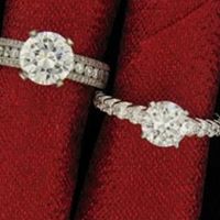
Phoenix Jeweler Jay Goldman
view source
Jay Goldman
view source
Jay Goldman
view source
Jay Goldman
view source
Jay Goldman
view source
Jay Goldman
view source
Jay Goldman
view source
Jay Goldman
view sourceGoogleplus

Jay Goldman
Work:
Klick - VP Strategy
Rypple - Head of Marketing
Radiant Core - President
Rypple - Head of Marketing
Radiant Core - President
Education:
University of Guelph - Information Systems and Human Behaviour
Tagline:
Technologist, designer, author, speaker, generally swell guy.

Jay Goldman
Work:
Euro Drive - Promotions (2010-2012)
Tagline:
Www.eurodrive.tv productions
Jay Goldman

Jay Goldman

Jay Goldman

Jay Goldman
Jay Goldman

Jay Goldman
Youtube
Myspace
Flickr
Get Report for Jay L Goldman from Mountain View, CA, age ~71


