Jie Chen
age ~43
from Missouri City, TX
Jie Chen Phones & Addresses
- Missouri City, TX
- Plano, TX
- Dallas, TX
Us Patents
-
Phenylenediamine Urotensin-Ii Receptor Antagonists And Ccr-9 Antagonists
view source -
US Patent:7288538, Oct 30, 2007
-
Filed:Aug 23, 2004
-
Appl. No.:10/924180
-
Inventors:Chengde Wu - Pearland TX, US
Daxin Gao - Houston TX, US
Ronald Biediger - Houston TX, US
Jie Chen - Houston TX, US
Robert V. Market - Pearland TX, US -
Assignee:Encysive Pharmaceuticals, Inc. - Houston TX
-
International Classification:A61K 31/5375
A61K 31/4523
A61K 31/4025
A61K 31/381
C07D 413/10
C07D 409/10 -
US Classification:51421019, 5142315, 514326, 514422, 514444, 544146, 546213, 548527, 548950, 549 59, 549 60
-
Abstract:The present invention relates to urotensin II receptor antagonists, CCR-9 antagonists, pharmaceutical compositions containing them and their use.
-
Phenylenediamine Urotensin-Ii Receptor Antagonists And Ccr-9 Antagonists
view source -
US Patent:7579340, Aug 25, 2009
-
Filed:Aug 22, 2007
-
Appl. No.:11/895069
-
Inventors:Ronald Biediger - Houston TX, US
Jie Chen - Houston TX, US
Daxin Gao - Houston TX, US
Robert Market - Pearlman TX, US
Chengde Wu - Pearland TX, US -
Assignee:Pfizer Inc - New York NY
-
International Classification:A61K 31/5375
A61K 31/4523
A61K 31/4025
A61K 31/381
C07D 413/10
C07D 409/10 -
US Classification:51421019, 5142315, 514326, 514422, 514444, 544146, 546213, 548527, 548950, 549 59, 549 60
-
Abstract:The present invention relates to urotensin II receptor antagonists, CCR-9 antagonists, pharmaceutical compositions containing them and their use.
-
Modulators Of Ccr9 Receptor And Methods Of Use Thereof
view source -
US Patent:8178699, May 15, 2012
-
Filed:Jul 30, 2008
-
Appl. No.:12/183032
-
Inventors:Eric C Anderson - Irving TX, US
Ronald J Biediger - Houston TX, US
Jie Chen - Houston TX, US
Brian Dupre - Houston TX, US
Pedro Lory - Antwerp, BE
Robert V. Market - Pearland TX, US
Keith A. Monk - League City TX, US
Michael M. Savage - Pearland TX, US
Reginald Tennyson - Missouri City TX, US
Brandon M. Young - Germantown TN, US -
Assignee:Pfizer Inc. - New York NY
-
International Classification:C07D 333/56
-
US Classification:549 57
-
Abstract:Provided are compounds that are modulators of CCR9 receptor activity, compositions containing the compounds and methods of use of the compounds and compositions. In certain embodiments, provided are methods for treating or ameliorating diseases associated with modulation of CCR9 receptor activity.
-
Modulators Of C3A Receptor And Methods Of Use Thereof
view source -
US Patent:20080188528, Aug 7, 2008
-
Filed:Dec 21, 2007
-
Appl. No.:12/004956
-
Inventors:Ronald J. Biediger - Houston TX, US
Huong M. Bui - Pearland TX, US
Jie Chen - Houston TX, US
Kevin M. Henry - Pearland TX, US
Thomas Thrash - Houston TX, US -
International Classification:A61K 31/4439
C07D 213/02
A61K 31/44
A61K 31/381
A61K 31/34
A61P 25/00
A61P 31/00
A61P 15/08
A61P 9/00
C07D 307/34
C07D 333/02
A61K 31/19 -
US Classification:514341, 546298, 514350, 514557, 562400, 5462747, 549 29, 514438, 549487, 514461
-
Abstract:Provided are compounds that are modulators of C3a receptor activity, compositions containing the compounds and methods of use of the compounds and compositions. In certain embodiments, the compounds are pyridones. In certain embodiments, provided are methods for treatment or amelioration of diseases associated with modulation of C3a receptor activity.
-
Semiconductor Package With Shunt And Patterned Metal Trace
view source -
US Patent:20220384353, Dec 1, 2022
-
Filed:Oct 13, 2021
-
Appl. No.:17/500086
-
Inventors:- Dallas TX, US
Rajen Manicon Murugan - Dallas TX, US
Liang Wan - Chengdu, CN
Makarand Ramkrishna Kulkarni - Dallas TX, US
Jie Chen - Plano TX, US
Steven Alfred Kummerl - Carrollton TX, US -
International Classification:H01L 23/538
H01L 23/00
H01L 21/48 -
Abstract:A semiconductor package includes a first layer including a semiconductor die and a shunt embedded within a first dielectric substrate layer, and metal pillars extending therethrough. The semiconductor package further includes a second layer stacked on the first layer, the second layer including a metal trace patterned on the first dielectric substrate layer, and a second dielectric substrate layer over the metal trace. The metal trace electrically connects a first portion of the shunt to a first metal pillar of the metal pillars and electrically connects a second portion of the shunt to a second metal pillar of the metal pillars. The semiconductor package further includes a base layer opposite the second layer relative the first layer, the base layer forming exposed electrical contact pads for the semiconductor package, the electrical contact pads providing electrical connections to the shunt, the metal pillars, and the semiconductor die.
-
Passives To Facilitate Mold Compound Flow
view source -
US Patent:20230101847, Mar 30, 2023
-
Filed:Sep 30, 2021
-
Appl. No.:17/491378
-
Inventors:- Dallas TX, US
Yiqi TANG - Allen TX, US
Rajen Manicon MURUGAN - Dallas TX, US
Jie CHEN - Plano TX, US
Tianyi LUO - Allen TX, US -
International Classification:H01L 25/065
H01L 23/31
H01L 23/00
H01L 23/498
H01L 25/00
H01L 21/56 -
Abstract:In examples, a semiconductor package comprises a substrate and multiple columns of semiconductor dies positioned approximately in parallel along a length of the substrate. The package also includes multiple passive components positioned between the multiple columns of semiconductor dies, the multiple passive components angled between 30 and 60 degrees relative to the length of the substrate, a pair of the multiple passive components having a gap therebetween that is configured to permit mold compound flow through capillary action. The package also includes a mold compound covering the substrate, the multiple columns of semiconductor dies, and the multiple passive components.
-
Semiconductor Device With A Multilayer Package Substrate
view source -
US Patent:20230021179, Jan 19, 2023
-
Filed:Jul 19, 2021
-
Appl. No.:17/379549
-
Inventors:- Dallas TX, US
Rajen Manicon Murugan - Dallas TX, US
Chittranjan Mohan Gupta - Richardson TX, US
Jie Chen - Plano TX, US -
International Classification:H01L 49/02
H01F 17/00
H05K 3/46
H05K 1/11
H02M 3/158 -
Abstract:A semiconductor device includes a die having an input port and an output port. The semiconductor device also includes a multilayer package substrate with pads on a surface of the multilayer package substrate configured to be coupled to circuit components of a printed circuit board. The multilayer package substrate also includes a passive filter comprising an input port and an output port, and a planar inductor. The planar inductor is coupled to a given pad of the pads of the multilayer package substrate with a first via of the multilayer package substrate and to the input port of the die with a second via of the multilayer package substrate. The planar inductor extends parallel to the surface of the multilayer package substrate.
-
Hall-Effect Sensor Package With Added Current Path
view source -
US Patent:20210159403, May 27, 2021
-
Filed:Jan 6, 2021
-
Appl. No.:17/142539
-
Inventors:- Dallas TX, US
Yiqi Tang - Allen TX, US
Jie Chen - Dallas TX, US
Enis Tuncer - Dallas TX, US
Usman Mahmood Chaudhry - McKinney TX, US
Tony Ray Larson - Tucson AZ, US
Rajen Manicon Murugan - Dallas TX, US
John Paul Tellkamp - Rockwall TX, US
Satyendra Singh Chauhan - Murphy TX, US -
International Classification:H01L 43/14
H01L 43/06
G01R 15/20
H01L 23/495
G01R 33/07 -
Abstract:A Hall-effect sensor package includes and an IC die including a Hall-Effect element and a leadframe including leads on a first side providing a first field generating current (FGC) path including ≥1 first FGC input pin coupled by a reduced width first curved head over or under the Hall-effect sensor element to ≥1 first FGC output pin, and second leads on a second side of the package. Some leads on the second side are attached to bond pads on the IC die including the output of the Hall-effect element. A clip is attached at one end to the first FGC input pin and at another end to a location on the first FGC output pin, having a reduced width second curved head in between that is over or under the Hall-effect sensor element opposite the first head.
Lawyers & Attorneys

Jie Chen - Lawyer
view sourceAddress:
Jun He Law Offices
85191300xx (Office)
85191300xx (Office)
Licenses:
New York - Currently registered 2005
Education:
Columbia Law School

Jie Chen - Lawyer
view sourceAddress:
Chen, Jie
7038070555 (Office)
7038070555 (Office)
Licenses:
New York - Delinquent 2002
Education:
The George Washington University

Jie Chen - Lawyer
view sourceAddress:
Volkswagen (China) Investment Company Limited
1065313067 (Office)
1065313067 (Office)
Licenses:
New York - Currently registered 2008
Education:
Columbia Law School

Jie Chen - Lawyer
view sourceAddress:
Nanjing University of Finance & Economics School of Law
2552268189 (Office)
2552268189 (Office)
Licenses:
New York - Currently registered 2011
Education:
University of Connecticut School of Law

Jie Chen - Lawyer
view sourceSpecialties:
Debt Finance
Mergers and Acquisitions
Capital Markets
Corporate & Incorporation
Banking
Contracts & Agreements
Mergers and Acquisitions
Capital Markets
Corporate & Incorporation
Banking
Contracts & Agreements
ISLN:
920304141
Admitted:
2006
University:
Concord College, B.S., 1999; Concord College, B.S., 1999
Law School:
University of Michigan, J.D., 2005

Jie Chen - Lawyer
view sourceOffice:
Jun He Law Offices
ISLN:
920593330
Admitted:
1994
University:
Tongji University, Shanghai, China,, B.S.
Law School:
Columbia University School of Law, New York, New York, U.S.A.,, LL.M.; Fudan University School of Law, Shanghai, China,, LL.B.
Wikipedia References

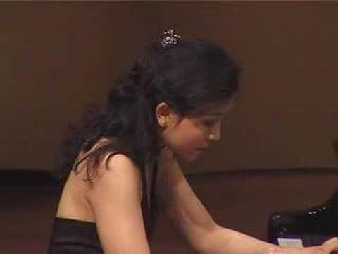
Jie Chen (Pianist)

Jie Chen (Statistician)
Resumes

Jie Chen Houston, TX
view sourceWork:
Brock Enterprises LLC
2012 to 2000
Designer Thermon Manufacturing
2011 to 2011
Designer (Contract) The Gardens Apartments
2011 to 2011
Accounting Clerk (Contract) Englobal Engineering Inc
2007 to 2009
CAD Operator
2012 to 2000
Designer Thermon Manufacturing
2011 to 2011
Designer (Contract) The Gardens Apartments
2011 to 2011
Accounting Clerk (Contract) Englobal Engineering Inc
2007 to 2009
CAD Operator
Education:
HCC
Houston, TX
2013 to 2014
Continuing Education in in Accounting University of Houston - Downtown
Houston, TX
2010 to 2011
BBA in Accounting
Houston, TX
2013 to 2014
Continuing Education in in Accounting University of Houston - Downtown
Houston, TX
2010 to 2011
BBA in Accounting
Skills:
Accounting: journal entries, accounts payable/receivable, adjusting entries, closing entries, federal income taxation, auditing, CPA candidate, business laws/regulations

Jie Chen Seattle, WA
view sourceWork:
Joint position by Purdue University and Total
West Lafayette, IN
Oct 2013 to Oct 2015
Industrial Postdoc Research Associate Schlumberger-Doll Research
Cambridge, MA
Jun 2013 to Oct 2013
Internship University of Washington
Seattle, WA
Oct 2010 to Jun 2013
Research Assistant University of Washington
Houston, TX
Jun 2012 to Sep 2012
Internship Georgia Southern University
Statesboro, GA
2008 to 2009
Research Assistant
Education:
University of Washington
Seattle, WA
2009 to 2013
Ph.D in Department of Mathematics Georgia Southern University
May 2009
M.Sc. in Mathematical Science Zhejiang University
Hangzhou, CN
2003 to 2007
B.S. in Applied Math
Seattle, WA
2009 to 2013
Ph.D in Department of Mathematics Georgia Southern University
May 2009
M.Sc. in Mathematical Science Zhejiang University
Hangzhou, CN
2003 to 2007
B.S. in Applied Math

Jie Chen San Jose, CA
view sourceWork:
Tibco Software Inc
Palo Alto, CA
Nov 2012 to Jun 2013
GL Accountant (Contractor) Occidental Petroleum Corporation
Houston, TX
Jun 2010 to Sep 2012
Financial Reporting Accountant COSL Drilling Pan-Pacific Ltd (parent company of Premium Driling Inc.)
Singapore
Jun 2009 to Dec 2009
Internal Consultant Premium Drilling Inc. (the company was dissolved in June 2009)
Houston, TX
Sep 2006 to Jun 2009
Senior Accountant Noble Corporation
Sugar Land, TX
Jun 2004 to Sep 2006
Staff Accountant Foxconn Corporation
Houston, TX
Apr 2003 to Jun 2004
Accounts Payable Specialist
Education:
University of Houston
Houston, TX
Dec 2002
Bachelor of Business Administration in Accounting
Houston, TX
Dec 2002
Bachelor of Business Administration in Accounting
Skills:
Proficient in Oracle R12 & 11i, Hyperion Financial Management, Hyperion Enterprise, Blackline Systems, experienced with SAP, JD Edwards, proficient in Excel, Access, Word, Outlook

Jie Chen Seattle, WA
view sourceWork:
WesternGeco, Schlumberger
Houston, TX
Jun 2012 to Sep 2012
Internship University of Washington
Seattle, WA
2011 to 2012
Research Assistant Georgia Southern University
Statesboro, GA
2008 to 2009
Research Assistant
Houston, TX
Jun 2012 to Sep 2012
Internship University of Washington
Seattle, WA
2011 to 2012
Research Assistant Georgia Southern University
Statesboro, GA
2008 to 2009
Research Assistant
Education:
Georgia Southern University
May 2009
M.Sc. in Department of Mathematical Science University of Washington
Ph.D in Department of Mathematics
May 2009
M.Sc. in Department of Mathematical Science University of Washington
Ph.D in Department of Mathematics
Skills:
Geophysical inverse problems, migarition, Seismic tomography, Mathematical modeling, numerical algorithm, optimization, statistics, dada analysis, operation research, MATLAB/C++ programming

Jie Chen West Lafayette, IN
view sourceWork:
Geo-Mathematical Imaging Group, Dept. of Math, Purdue University
Oct 2013 to 2000
Industrial Postdoc Research Associate funded by Total Schlumberger-Doll Research
Cambridge, MA
Jun 2013 to Oct 2013
Internship University of Washington
Seattle, WA
Oct 2010 to Jun 2013
Research Assistant WesternGeco, Schlumberger
Houston, TX
Jun 2012 to Sep 2012
Internship Georgia Southern University
Statesboro, GA
2008 to 2009
Research Assistant
Education:
University of Washington
Seattle, WA
2009 to 2013
Ph.D in Department of Mathematics Georgia Southern University
May 2009
M.Sc. in Department of Mathematical Science Zhejiang University
Hangzhou, China
2003 to 2007
BS in Applied math
Seattle, WA
2009 to 2013
Ph.D in Department of Mathematics Georgia Southern University
May 2009
M.Sc. in Department of Mathematical Science Zhejiang University
Hangzhou, China
2003 to 2007
BS in Applied math
Skills:
Mathematical analysis, algorithm development, numerical analysis, mathematical modeling, numerical inversion, optimization, geophysical interpretation, high performance computing with MPI, CSEM, FWI; Matlab, fortran, python, C/C++
Isbn (Books And Publications)

Ideology in U. S. Foreign Policy: Case Studies in U. S.-China Policy
view sourceAuthor
Jie Chen
ISBN #
0275943275

China Since the Cultural Revolution: From Totalitarianism to Authoritarianism
view sourceAuthor
Jie Chen
ISBN #
0275946479


Design of Digital Video Coding Systems: A Complete Compressed Domain Approach
view sourceAuthor
Jie Chen
ISBN #
0824706560

Name / Title
Company / Classification
Phones & Addresses
RAY KANG INVESTMENT LLC
727 Bunker Hl Rd APT 92, Houston, TX 77024
CHINA LONGYI GROUP INTERNATIONAL HOLDINGS LIMITED
Director, President
Chen's Hong Yun Corporation
8376 Leamont Dr, Houston, TX 77072
Manager
CLARIN ENTERPRISE, LLC
Business Services
Business Services
8912 Chancellor Row, Dallas, TX 75247
Medicine Doctors

Jie Chen
view sourceSpecialties:
Transplant Surgery
Work:
University Of Virginia Transplant Center
1300 Jefferson Park Ave FL 4, Charlottesville, VA 22903
4349248604 (phone), 4349240017 (fax)
UVA Medical Center Inpatient Transplant Surgery & Urology
1215 Lee St 5 W, Charlottesville, VA 22908
4349242338 (phone), 4349242355 (fax)
1300 Jefferson Park Ave FL 4, Charlottesville, VA 22903
4349248604 (phone), 4349240017 (fax)
UVA Medical Center Inpatient Transplant Surgery & Urology
1215 Lee St 5 W, Charlottesville, VA 22908
4349242338 (phone), 4349242355 (fax)
Languages:
English
Description:
Ms. Chen works in Charlottesville, VA and 1 other location and specializes in Transplant Surgery. Ms. Chen is affiliated with University Of Virginia Medical Center.

Jie Chen
view sourceYoutube
Myspace

Jie Chen
view source
Jie Chen
view sourceClassmates

Jie Chen
view sourceSchools:
Nido De Aguilas High School Santiago Chile 1990-1994
Community:
Joy Fox, Lisa Ireland

Jie Chen
view sourceSchools:
Remington Elementary School Ilion NY 2000-2004
Community:
David Wickersham, Chris Walsh, Jessica Elthorp, Kari Holtz, Jared Hoffman

Jie Chen
view sourceSchools:
City Adult Learning Center School Toronto Morocco 1994-1998

Jun Jie Chen, Edgewater H...
view source
Remington Elementary Scho...
view sourceGraduates:
Jennifer Wheelock (2000-2004),
Marda Gaines (1975-1979),
Meghan McKenney (1992-1997),
Wendy Smith (1986-1986),
Jie Chen (2000-2004)
Marda Gaines (1975-1979),
Meghan McKenney (1992-1997),
Wendy Smith (1986-1986),
Jie Chen (2000-2004)

University of Delaware, N...
view sourceGraduates:
Dhaval Mavani (2003-2007),
Rick Bradley (1974-1978),
Jie Chen (1993-1997),
Melinda Bush (1977-1981)
Rick Bradley (1974-1978),
Jie Chen (1993-1997),
Melinda Bush (1977-1981)

University of Toronto - E...
view sourceGraduates:
Bruce Robinson (1954-1959),
Jim Kenning (1977-1981),
Jie Chen (1998-2002),
Terry Jacobs (1958-1962),
Susan Oh (1998-2003)
Jim Kenning (1977-1981),
Jie Chen (1998-2002),
Terry Jacobs (1958-1962),
Susan Oh (1998-2003)
News

Could LLMs help design our next medicines and materials?
view source- atusik, a professor of electrical engineering and computer science at MIT who leads the Computational Design and Fabrication Group within the Computer Science and Artificial Intelligence Laboratory (CSAIL); Meng Jiang, associate professor at the University of Notre Dame; and senior author Jie Chen,
- Date: Apr 09, 2025
- Category: Science
- Source: Google
Plaxo

chen jie
view sourceCHINAHi, I am sophie from china ,happy to you and me being friend !

Jie Chen
view sourceMountain View, CA

Jie Chen
view sourceKunde
Flickr
Googleplus

Jie Chen
Work:
BUPT - Lecturer (2007)
Starpoint - PM (2007)
Starpoint - PM (2007)
Education:
BUPT - Circuits and Systems

Jie Chen
Work:
OmarTech - Boss
Education:
Beijing Institute of Technology

Jie Chen

Jie Chen
Education:
Macquarie university - Accounting, Nanjing foreign language school

Jie Chen

Jie Chen
Education:
New York City College of Technology - Advertising Deisgn

Jie Chen

Jie Chen
Bragging Rights:
学生党

Jie Chen Lansing / East ...
view sourceJie Chen (Lansing / East Lansing, MI)

Jie Chen Orange County CA
view sourceFriends:
Hao Tan, Peter Ant, Di Wang, Chenwei Wang, Zheng Kevin
Jie Chen (Orange County, CA)

Wen Jie Chen Xu Colombia
view sourceFriends:
Cristian Vasquez, Esmeralda Arboleda Prez, Elizabeth Velasquez
Wen Jie Chen Xu (Colombia)

Jie Chen Ld
view sourceFriends:
Hong Ding, Jeffrey Jiang, Angelia Abad, Monica Liang, Lisa Li
Jie Chen (London)

Moses Ying Jie Chen Hg Kg
view sourceFriends:
Augustus Cheung, Kary Ho, Yiu Kan Lam
Moses Ying Jie Chen (Hong Kong)

Jie Chen Ann Arbor MI
view sourceFriends:
Mengfei Sun, Jacqueline Liu, Zhengxu Wang, Lisa Li
Jie Chen (Ann Arbor, MI)

Jie Liang Chen
view source
Jie Chen
view sourceGet Report for Jie Chen from Missouri City, TX, age ~43


