Joan S Gray
age ~76
from Herndon, VA
- Also known as:
-
- Joan K Gray
- Jaon S Gray
- Phone and address:
-
1405 Bakers Creek Ct, Herndon, VA 20170
7034301927
Joan Gray Phones & Addresses
- 1405 Bakers Creek Ct, Herndon, VA 20170 • 7034301927
- Fernandina Beach, FL
- Corolla, NC
- Old Bridge, NJ
Work
-
Company:Pcc stride inc2012
-
Position:Activities therapist/placement supervisor full-time
Education
-
School / High School:Coppin State College/University of Baltimore- Baltimore, MD2002
-
Specialities:Master of Science in Human Services Administration and Drug & Alcohol Counseling
Lawyers & Attorneys

Joan Gray - Lawyer
view sourceISLN:
906922352
Admitted:
1983
University:
Bernard M. Baruch College of the City University of New York, M.P.A., 1978; State University of New York at Oswego, B.A., 1970
Law School:
St. John's University, J.D., 1982
Wikipedia References

Joan Gray
Name / Title
Company / Classification
Phones & Addresses
Principal
George E Wilson Elem School
Elementary and Secondary Schools
Elementary and Secondary Schools
600 E Park Ave, Trenton, NJ 08610
Website: hamilton.k12.nj.us
Website: hamilton.k12.nj.us
Finance Executive
Tru Limousine
Local Passenger Transportation
Local Passenger Transportation
41 W Edgar Rd, Tremley, NJ 07036
Principal
George E Wilson Elem School
Elementary & Secondary Schools
Elementary & Secondary Schools
600 E Park Ave, Trenton, NJ 08610
6096314169, 6095815054
6096314169, 6095815054
Director Of Communications
Beth Israel Medical Center (inc)
3201 Kings Hwy, Brooklyn, NY 11234
7182523000, 7182526101
7182523000, 7182526101
Resumes

Joan Gray Springdale, MD
view sourceWork:
PCC Stride Inc
2012 to 2000
Activities Therapist/Placement Supervisor Full-time J.P. Gray and Associates, Inc
2005 to 2000
President and CEO J.P. Gray and Associates, Inc
2005 to 2000
Adjunct Faculty United States Department of Education
2003 to 2000
Grant Reviewer Psychiatric Centered Charter, Inc./Stride, Inc
Washington, DC
2006 to 2012
Activities Therapist/Program Assistant Institute for Behavioral Change and Research
Washington, DC
2002 to 2006
Pro-Social Family Therapist (Part-Time) Baltimore City Department of Social Services
Baltimore, MD
2000 to 2002
Family Services Case Worker II Stevenson and Associates
Columbia, MD
2000 to 2001
Psychiatric Rehabilitation Counselor (Part-Time) University of Maryland at Baltimore Center for Infant Studies
Baltimore, MD
1998 to 2000
Mental Health Coordinator Awele Treatment and Rehabilitation Services
Baltimore, MD
1997 to 1998
Director of Family Services Oakview Treatment and Rehabilitation Center
Ellicott City, MD
1996 to 1997
Psychiatric Rehabilitation Counselor (Part-Time) United States Army/Reserve
Fort Meade, MD
1975 to 1986
Various Positions
Education:
Coppin State College/University of Baltimore
Baltimore, MD
2002
Master of Science in Human Services Administration and Drug & Alcohol Counseling Coppin State College
Baltimore, MD
1996
Bachelor of Science in Psychology Anne Arundel Community College
1994
Associate of Arts in General Studies
Baltimore, MD
2002
Master of Science in Human Services Administration and Drug & Alcohol Counseling Coppin State College
Baltimore, MD
1996
Bachelor of Science in Psychology Anne Arundel Community College
1994
Associate of Arts in General Studies
Isbn (Books And Publications)


License Records
Joan A Gray
License #:
RS143946A - Expired
Category:
Real Estate Commission
Type:
Real Estate Salesperson-Standard
Us Patents
-
Field Emitter Cell And Array With Vertical Thin-Film-Edge Emitter
view source -
US Patent:20020190622, Dec 19, 2002
-
Filed:Jun 13, 2001
-
Appl. No.:09/883458
-
Inventors:David Hsu - Alexandria VA, US
Henry Gray - Alexandria VA, US
Joan Gray - Alexandria VA, US
James Gray - , US -
International Classification:H01J001/304
H01J019/24 -
US Classification:313/309000
-
Abstract:A field emitter cell includes a thin film edge emitter normal to a gate layer. The field emitter is a multilayer structure including a low work function material sandwiched between two protective layers. The field emitter may be fabricated from a composite starting structure including a conductive substrate layer, an insulation layer, a standoff layer and a gate layer, with a perforation extending from the gate layer into the substrate layer. The emitter material is conformally deposited by chemical beam deposition along the sidewalls of the perforation. Alternatively, the starting material may be a conductive substrate having a protrusion thereon. The emitter layer, standoff layer, insulation layer, and gate layer are sequentially deposited, and the unwanted portions of each are preferentially removed to provide the desired structure.
Flickr
Myspace
Googleplus
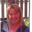
Joan Gray
Relationship:
Single

Joan Gray

Joan Gray

Joan Gray

Joan Gray

Joan Gray

Joan Gray

Joan Gray
Classmates
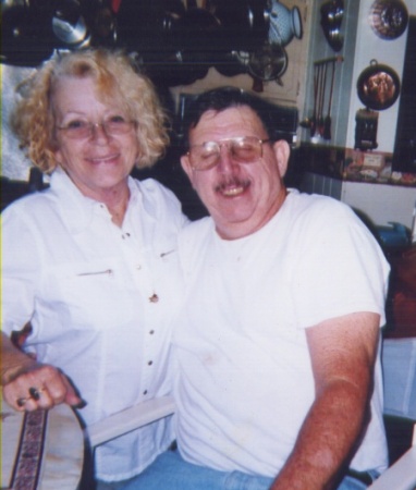
Joan Welborn (Gray)
view sourceSchools:
Desoto County High School Arcadia FL 1957-1961
Community:
Charles Beck, Cindy Sloan, Diane Barnard

Joan Harker (Gray)
view sourceSchools:
worthington high Worthington OH 1976-1980
Community:
Sue Wellman, Keith Garrard, Victor Liquori

Joan Gray (Roy)
view sourceSchools:
Sacred Heart Academy Bathurst NB 1948-1952
Community:
James Murphy, Carole Comeau

Joan Gray (Ryan)
view sourceSchools:
Galatia Community High School Galatia IL 1947-1951
Community:
Olen Butch, Sharlene Malone, Kenny Stevens, Ted Wallace, Connie Higgins

Joan Gray (Ryan)
view sourceSchools:
Galatia Community High School Galatia IL 1947-1951
Community:
Olen Butch, Sharlene Malone, Kenny Stevens, Ted Wallace, Connie Higgins

Joan Gray (Scott)
view sourceSchools:
St. Bartholomew School Chicago IL 1938-1946
Community:
Roberta Bobbee, Sarah Williams, Frank Giunta, Mary Bridges, Ralph Malec

Joan Gray
view sourceSchools:
Mt. Pleasant High School Mt. Pleasant OH 1950-1954
Community:
Chris Moffo, Leslie Sedgmer, Arlene Manbeck

Joan Riley (Gray)
view sourceSchools:
Sabina High School Sabina OH 1961-1965
Community:
Carolyn Gray, Connie Rice, Molly Iles
Youtube
Joan Engdahl Gray
view source
Lola Joan Gray
view source
Joan Brennan Gray
view source
Joan Gray Moore
view source
Joan Chatterson Gray
view source
Ellivia Joan Gray
view source
Joan Porter Gray
view source
Joan Solidum Gray
view sourceGet Report for Joan S Gray from Herndon, VA, age ~76


