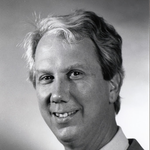
John W Atwood
age ~65
from Piru, CA
- Also known as:
-
- John Wesley Atwood
- John E Atwood
- John William Kemp Charleen
- Jrjohn W Atwood
- John W Kemp
- John W Otwood
- Christine Atwood
- John Watwood
- Esther Kitchen
John Atwood Phones & Addresses
- Piru, CA
- 3215 SW Cascade Ave, Corvallis, OR 97333 • 5419773890
- Ventura, CA
- Camarillo, CA
- Oxnard, CA
- Soledad, CA
Work
-
Position:Professional/Technical
Vehicle Records
-
John Atwood
view source -
Address:PO Box 764, Piru, CA 93040
-
Phone:8056254310
-
VIN:1GTHK29628E190883
-
Make:GMC
-
Model:SIERRA 2500HD
-
Year:2008
Lawyers & Attorneys

John F Atwood - Lawyer
view sourceLicenses:
Dist. of Columbia - Active 1986
Medicine Doctors

John Edwin Atwood
view sourceSpecialties:
Internal Medicine
Cardiovascular Disease
Cardiology
Cardiovascular Disease
Cardiology
Education:
Yale University (1975)
Isbn (Books And Publications)

The Tao of Universalism: The Thoughts, Teachings, and Writings of Dr. John Murray Atwood
view sourceAuthor
John Murray Atwood
ISBN #
0533082862
Name / Title
Company / Classification
Phones & Addresses
President
PAST, INC
Business Services at Non-Commercial Site · Nonclassifiable Establishments
Business Services at Non-Commercial Site · Nonclassifiable Establishments
18734 Nordhoff St, Northridge, CA 91324
Incorporator
FIRST LAMAR SAVINGS AND LOAN ASSOCIATION
President
TOWER T.V., INC
729 Portola Dr, San Francisco, CA 94127
President
BLUE TRUCK PRODUCTIONS, INCORPORATED
9135 Reseda Blvd STE 114, Northridge, CA 91324
Us Patents
-
Printing Portable-Selected Information
view source -
US Patent:7006242, Feb 28, 2006
-
Filed:Oct 22, 2001
-
Appl. No.:10/045945
-
Inventors:Aloke Gupta - Corvallis OR, US
Charlie Udom - Corvallis OR, US
John Atwood - Corvallis OR, US
Keith M. Taylor - Corvallis OR, US
William P. Brown - Portland OR, US -
Assignee:Hewlett-Packard Development Company, L.P. - Houston TX
-
International Classification:G06K 15/00
-
US Classification:358 115, 358 16
-
Abstract:A user of a portable device may request a full-length information set be sent to a high capacity presentation apparatus for printing. A truncated or compressed information set is displayed on the portable device, which the user may select for later printing of the full-length information on the high capacity presentation apparatus when the portable device is synchronized.
-
Versatile Printing From Portable Electronic Device
view source -
US Patent:20030020954, Jan 30, 2003
-
Filed:Jul 26, 2001
-
Appl. No.:09/917016
-
Inventors:Charlie Udom - Albany OR, US
John Atwood - Corvallis OR, US
Keith Taylor - Corvallis OR, US
William Brown - Portland OR, US -
International Classification:G06F015/00
B41J001/00 -
US Classification:358/001180, 358/001150
-
Abstract:Printing is performed from a portable device. Upon a selection to print, available printing options are displayed. This includes providing an option to print remote data accessible at a location outside of the portable device by reference to the location outside of the portable device. Upon selection of one of the available printing options, a print operation is performed in accordance with the selection.
-
Method And Apparatus For Writing To Memory Components
view source -
US Patent:56803613, Oct 21, 1997
-
Filed:Feb 14, 1995
-
Appl. No.:8/389561
-
Inventors:Frederick A. Ware - Los Altos CA
John B. Dillon - Palo Alto CA
Richard M. Barth - Palo Alto CA
Billy Wayne Garrett - Mountain View CA
John Girdner Atwood - San Jose CA
Michael P. Farmwald - Portola Valley CA
Richard DeWitt Crisp - Cupertino CA -
Assignee:Rambus, Inc. - Mountain View CA
-
International Classification:G11C 11401
-
US Classification:36523001
-
Abstract:Additional modes are provided to enhance the functionality and performance of a memory system. In one embodiment, a unique bit mask is supplied with the write data used in each column access. In an alternate embodiment, a bit mask register and byte mask register are provided to support bit level and byte level masking. The bit mask and write data registers are realized as a single register to provide the functionality while minimizing component space and cost. In another embodiment, a separate bit mask and byte mask are provided. The byte mask is loaded with mask data in one cycle and is used during the next "q" column write accesses. This structure provides for operating modes with no bit masking, with bit masks supplied for every row access, and with bit masks supplied with every column access. In order to enhance the functionality of a system, such as a two-dimensional graphics system, in an alternate embodiment, the memory system is provided with two registers and a select control line to select data from one of two registers. In a computer graphics system, this is used to select between foreground and background colors.
-
Method And Apparatus For Writing To Memory Components
view source -
US Patent:59403403, Aug 17, 1999
-
Filed:May 16, 1997
-
Appl. No.:8/858068
-
Inventors:Frederick A. Ware - Los Altos CA
John B. Dillon - Palo Alto CA
Richard M. Barth - Palo Alto CA
Billy Wayne Garrett - Mountain View CA
John Girdner Atwood - San Jose CA
Michael P. Farmwald - Portola Valley CA
Richard DeWitt Crisp - Cupertino CA -
Assignee:Rambus, Inc. - Mountain View CA
-
International Classification:G11C 11401
-
US Classification:36523001
-
Abstract:Additional operating modes are provided to enhance the functionality and performance of a memory system. In one embodiment, a unique bit mask is supplied with the write data used in each column access. In an alternate embodiment, a bit mask register and byte mask register are provided to support bit level and byte level masking. The bit mask and write data registers are realized as a single register to provide the functionality while minimizing component space and cost. In another embodiment, a separate bit mask and byte mask are provided. The byte mask is loaded with mask data in one cycle and is used during the next "q" column write accesses. This structure provides for operating modes with no bit masking, with bit masks supplied for every row access, and with bit masks supplied with every column access. In order to enhance the functionality of a system, such as a two-dimensional graphics system, in an alternate embodiment, the memory system is provided with two registers and a select control line to select data from one of two registers. In a computer graphics system, this is used to select between foreground and background colors.
-
Dynamic Random Access Memory System
view source -
US Patent:54306760, Jul 4, 1995
-
Filed:Feb 25, 1994
-
Appl. No.:8/202290
-
Inventors:Frederick A. Ware - Los Altos Hills CA
John B. Dillon - Palo Alto CA
Richard M. Barth - Palo Alto CA
Billy W. Garrett - Mountain View CA
John G. Atwood - San Jose CA
Michael P. Farmwald - Portola Valley CA -
Assignee:Rambus, Inc. - Mountain View CA
-
International Classification:G06F 1200
-
US Classification:36518902
-
Abstract:As interfaces to DRAMs become more advanced and higher performance, the interfaces and signal lines required to support the interface become more expensive to implement. Therefore, it is desirable to minimize the number of signal lines and maximize the bandwidth of the signal lines interfacing to the DRAM in order to take advantage of the high performance of the signal lines in the interface. In the DRAM memory system of the present invention, the address and control lines and are combined and the information multiplexed such that the DRAM pins have roughly equal information rate at all times.
-
Dynamic Random Access Memory System
view source -
US Patent:55110240, Apr 23, 1996
-
Filed:Feb 25, 1994
-
Appl. No.:8/201981
-
Inventors:Frederick A. Ware - Los Altos Hills CA
John B. Dillon - Palo Alto CA
Richard M. Barth - Palo Alto CA
Billy W. Garrett - Mountain View CA
John G. Atwood - San Jose CA
Michael P. Farmwald - Portola Valley CA -
Assignee:Rambus, Inc. - Mountain View CA
-
International Classification:G06F 112
-
US Classification:36518904
-
Abstract:As interfaces to DRAMs become more advanced and higher performance, the interfaces and signal lines required to support the interface become more expensive to implement. Therefore, it is desirable to minimize the number of signal lines and maximize the bandwidth of the signal lines interfacing to the DRAM in order to take advantage of the high performance of the signal lines in the interface. In the DRAM memory system of the present invention, the address and control lines and are combined and the information multiplexed such that the DRAM pins have roughly equal information rate at all times.
-
Multiple Power Supply Sensor For Protecting Shared Processor Buses
view source -
US Patent:50364553, Jul 30, 1991
-
Filed:Jul 25, 1989
-
Appl. No.:7/385330
-
Inventors:John G. Atwood - San Jose CA
-
Assignee:Tandem Computers Incorporated - Cupertino CA
-
International Classification:G06F 1130
-
US Classification:364200
-
Abstract:A multiple power supply sensor for protecting shared processor buses in a multiprocessor system. In the case that a power failure or power supply malfunction occurs in one of the processors of the system, at least one of the shared processor buses will be isolated from the malfunctioning processor. As a result, data on that bus is not corrupted by the manfunctioning processor. The isolation is accomplished by independent sensor circuits present in each processor for each bus.
-
Dynamic Random Access Memory System
view source -
US Patent:54348170, Jul 18, 1995
-
Filed:Nov 3, 1994
-
Appl. No.:8/333869
-
Inventors:Frederick A. Ware - Los Altos Hills CA
John B. Dillon - Palo Alto CA
Richard M. Barth - Palo Alto CA
Billy W. Garrett - Mountain View CA
John G. Atwood - San Jose CA
Michael P. Farmwald - Portola Valley CA -
Assignee:Rambus, Incorporated - Mountain View CA
-
International Classification:G11C 700
G06F 1206 -
US Classification:36518901
-
Abstract:As interfaces to DRAMs become more advanced and higher performance, the interfaces and signal lines required to support the interface become more expensive to implement. Therefore, it is desirable to minimize the number of signal lines and maximize the bandwidth of the signal lines interfacing to the DRAM in order to take advantage of the high performance of the signal lines in the interface. In the DRAM memory system of the present invention, the address and control lines and are combined and the information multiplexed such that the DRAM pins have roughly equal information rate at all times.
Classmates

John Atwood
view sourceSchools:
Cady Elementary School Wayne MI 1958-1962, Taft - Galloway Elementary School Wayne MI 1962-1965, Franklin Junior High School Wayne MI 1965-1968
Community:
Ronald Triplett, Debra Oppenhein, Michael Macblain, Timothy Cook

John Atwood
view sourceSchools:
Lumberton High School Lumberton MS 1952-1956
Community:
Rebecca Hamersly

John Atwood (John (Bill) ...
view sourceSchools:
Lumberton High School Lumberton MS 1952-1956
Community:
Rebecca Hamersly

John Atwood
view sourceSchools:
Waldorf High School Bethesda MD 1991-1999
Community:
Valerie Forconi, Kate O'connor, Jerry Madden

John Atwood
view sourceSchools:
Kerens School Kerens TX 1958-1962
Community:
Micheal Wafford, Edwin Brown, Kim Webster, Nickey Andrews

John Atwood
view sourceSchools:
New York Vocational School New York NY 1969-1973
Community:
Anna Torres, Rogelio Archilla

John Atwood
view sourceSchools:
West Stokes High School King NC 1997-2001
Community:
Kimberly Finley, Erin Grady, Christy Moore, Valerie Coles

John Atwood
view sourceSchools:
Matoaka High School Matoaka WV 1961-1965
Community:
Warren Petris, Donna Gilley, Yuvonne Blankenship, Linda Johnson, Barbara White, Aletta Taylor, David Mckinney, Curtis Hurst, Diane Tilley, Goeorge Dillon, Judith Whitlow, Connie Delp
Youtube
Myspace
Googleplus

John Atwood
Lived:
Zurich, Switzerland
Berkeley, CA
San Francisco, CA
San Diego, CA
Dublin, Ireland
Rome Italy
Berkeley, CA
San Francisco, CA
San Diego, CA
Dublin, Ireland
Rome Italy
Work:
Google - Learning and Development Manager (2004)
Education:
Pepperdine University - Masters in Organization Development, UC San Diego - BA Communications and Theatre

John Atwood
Work:
State of New Mexico
Education:
University of New Mexico - Business
Tagline:
Retired and enjoying life

John Atwood
Tagline:
I am a consultant for start-up health clubs and turnarounds

John Atwood
Tagline:
Im sick of buying printer ink all the time.

John Atwood
Relationship:
Married

John Atwood

John Atwood

John Atwood

Land John Atwood
view sourceLandon John Atwood

John Atwood
view source
John Atwood
view source
John B Atwood
view source
'Atwood John
view source
John Atwood
view source
John J Atwood
view source
John Atwood Smith Jr
view sourceFlickr
Get Report for John W Atwood from Piru, CA, age ~65


