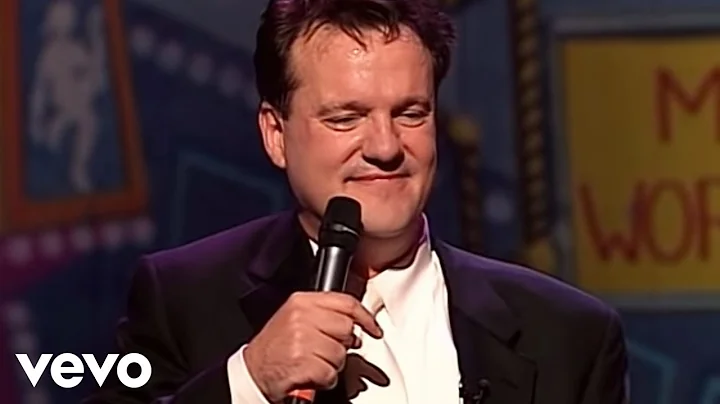
Mark C Lauer
age ~81
from Alameda, CA
- Also known as:
-
- Mark M Lauer
- Charles Mark Lauer
- Charles Te Lauer
- Charles M Lauer
- Liz Lauer
- Mark Lauer Cha
Mark Lauer Phones & Addresses
- Alameda, CA
- Westford, MA
- Walnut Creek, CA
- Santa Barbara, CA
- Carpinteria, CA
- Madison, CT
- Auburndale, MA
- Wallingford, CT
- 2310 State St, Santa Barbara, CA 93105 • 2032458297
Work
-
Company:D'elia associates of ct
-
Address:4 Laser Ln, Wallingford, CT 06492
-
Phones:2032940371
-
Position:Chief financial officer
-
Industries:Advertising
Education
-
School / High School:University of California - Davis
Ranks
-
Licence:California - Active
-
Date:1993
Resumes

Restaurant Manager At Latitude 28.02 Restaurant And Gallery
view sourcePosition:
Restaurant Manager at Ruggles Green
Location:
Rockport, Texas
Industry:
Restaurants
Work:
Ruggles Green - Houston, Texas since Jul 2011
Restaurant Manager
Whole Foods Market Jan 2010 - Jul 2011
Team Leader Prepared Foods
Key Allegro Yacht Club 2004 - Aug 2009
General Manager/F&B Director
Morton's of Chicago 2000 - 2004
Food and Beverage Manager
M.R. Lauer, Inc. dba Plaza Cafe 1992 - 2000
Owner/Manager
Restaurant Manager
Whole Foods Market Jan 2010 - Jul 2011
Team Leader Prepared Foods
Key Allegro Yacht Club 2004 - Aug 2009
General Manager/F&B Director
Morton's of Chicago 2000 - 2004
Food and Beverage Manager
M.R. Lauer, Inc. dba Plaza Cafe 1992 - 2000
Owner/Manager
Education:
Our Lady of the Lake University

Senior Pastor, Consultant, Coach, Spiritual Director
view sourcePosition:
Senior Pastor at Christ the King Anglican Church, Wedding Officiant and Pastor-at-large to the Community at Pastor Mark Lauer
Location:
San Francisco Bay Area
Industry:
Religious Institutions
Work:
Christ the King Anglican Church since Nov 2008
Senior Pastor
Pastor Mark Lauer since 2000
Wedding Officiant and Pastor-at-large to the Community
Calvary Church of Los Gatos Jul 2005 - Nov 2008
Pastor of Discipleship
Center for Relationship 2004 - 2008
Executive Vice-President and Co-founder
Menlo Park Presbyterian Church 2003 - 2004
Pastor of Single Adult Ministry
Education:
Santa Clara University 1994 - 1995
Fuller Theological Seminary 1986 - 1993
M.A., Theology Oregon State University 1983 - 1985
B.S., Psychology; Religious Studies minor Saratoga High School 1980
Fuller Theological Seminary 1986 - 1993
M.A., Theology Oregon State University 1983 - 1985
B.S., Psychology; Religious Studies minor Saratoga High School 1980
Skills:
Mentoring
Team Building
Creative Communication
Public Speaking
Coaching
Preaching
Leadership
Team Building
Creative Communication
Public Speaking
Coaching
Preaching
Leadership
Interests:
Family time, music, snow skiing, creative arts, travel around the world! sports

Partner At Silicon Edge Law Group Llp
view sourcePosition:
Partner at Silicon Edge Law Group LLP
Location:
San Francisco Bay Area
Industry:
Law Practice
Work:
Silicon Edge Law Group LLP
Partner
Partner
Education:
Thomas Jefferson School of Law

Mark Lauer
view sourceLocation:
United States
Lawyers & Attorneys
Mark Alan Lauer, Pleasanton CA - Lawyer
view sourceAddress:
Silicon Edge Law Group LLP
7901Stoneridge Dr Ste 528, Pleasanton, CA 94588
9256212121 (Office), 9256212119 (Fax)
7901Stoneridge Dr Ste 528, Pleasanton, CA 94588
9256212121 (Office), 9256212119 (Fax)
Licenses:
California - Active 1993
Education:
University of California - Davis
Thomas Jefferson School of Law
Thomas Jefferson School of Law
Specialties:
Intellectual Property - 100%

Mark Lauer - Lawyer
view sourceOffice:
Silicon Edge Law Group LLP
Specialties:
Intellectual Property Law
Business Law
Business Law
ISLN:
911764268
Admitted:
1993
University:
University of California, B.A.
Law School:
Thomas Jefferson School of Law, J.D.

Mark Lauer - Lawyer
view sourceOffice:
Samson Investment Co.
Specialties:
Oil and Gas Law
Employment Law
Business Law
Contracts
Securities
Employment Law
Business Law
Contracts
Securities
ISLN:
913102372
Admitted:
1992
University:
University of Oklahoma, B.A., 1989
Law School:
University of Oklahoma, J.D., 1992

Mark A. Lauer, Pleasanton CA - Lawyer
view sourceOffice:
Silicon Edge Law Group LLP
6601 Koll Center Pkwy., Ste. 245, Pleasanton, CA
6601 Koll Center Pkwy., Ste. 245, Pleasanton, CA
Specialties:
Intellectual Property Law
ISLN:
911764268
Admitted:
1993
University:
University of California, B.A.
Law School:
Thomas Jefferson School of Law, J.D.

Mark Alan Lauer, Pleasanton CA - Lawyer
view sourceAddress:
6601 Koll Center Pkwy, Pleasanton, CA 94566
Phone:
9254849295 (Phone), 9254849291 (Fax)
Experience:
32 years
Jurisdiction:
California (1993)
Law School:
Thomas Jefferson School of Law
Education:
Univ of California Davis, Undergraduate Degree
Thomas Jefferson School of Law, Law Degree
Thomas Jefferson School of Law, Law Degree
Memberships:
California State Bar (1993)
Medicine Doctors

Mark A. Lauer
view sourceSpecialties:
Occupational Medicine
Work:
Worknet Occupational Medicine
6301 Grayson Rd SPC 9, Harrisburg, PA 17111
7179205910 (phone), 7179205916 (fax)
6301 Grayson Rd SPC 9, Harrisburg, PA 17111
7179205910 (phone), 7179205916 (fax)
Education:
Medical School
Pennsylvania State University College of Medicine
Graduated: 1992
Pennsylvania State University College of Medicine
Graduated: 1992
Conditions:
Rheumatoid Arthritis
Systemic Lupus Erythematosus
Systemic Lupus Erythematosus
Languages:
English
Spanish
Spanish
Description:
Dr. Lauer graduated from the Pennsylvania State University College of Medicine in 1992. He works in Harrisburg, PA and specializes in Occupational Medicine.
Name / Title
Company / Classification
Phones & Addresses
Chief Financial Officer
D'Elia Associates of CT
Advertising
Advertising
4 Laser Ln, Wallingford, CT 06492
Co-Founder
Center for Relationship Abuse
Business Consulting Services
Business Consulting Services
555 Bryant St, Palo Alto, CA 94301
Executive Vice-President
Delia Inc
Mfg Household Appliances Whol Appliances/TV/Radio
Mfg Household Appliances Whol Appliances/TV/Radio
400 Blue Hl Dr, Islington, MA 02090
7813293347, 7813293110
7813293347, 7813293110
Partner
Silicon Edge Law Group
Legal Services, Nsk · Offices of Lawyers
Legal Services, Nsk · Offices of Lawyers
6601 Koll Ctr Pkwy, Pleasanton, CA 94566
9254612616, 9256212141, 9258374185, 9256212131
9254612616, 9256212141, 9258374185, 9256212131
Us Patents
-
Electromagnetic Heads, Flexures And Gimbals Formed On And From A Wafer Substrate
view source -
US Patent:6735049, May 11, 2004
-
Filed:Mar 28, 2002
-
Appl. No.:10/112004
-
Inventors:Mark A. Lauer - Pleasanton CA 94566
-
International Classification:G11B 2116
-
US Classification:3602441
-
Abstract:Devices for transducing electromagnetic information are formed on and from a wafer substrate. The devices comprise a head attached to a flexible element such as a gimbal. To create such a device, a transducer and an optional amplifier are formed on a wafer that is then cut into rows containing a number of such transducers. The rows are then processed from directions generally normal to the wafer surface upon which the transducer was formed, by removing material to form a head and flexible elements such as a gimbal, creating a media-facing surface on the head and at least one aperture adjacent the head. Conductive leads may be formed on a non-media-facing surface of a flexible element to connect the transducer with drive electronics. Conventional problems of connecting the head to the flexure and/or gimbal are eliminated, as both are made from the same wafer on which the transducer is formed. The transducer layers may be oriented generally perpendicular to the media surface, making use of proven transducer designs.
-
Integrated Optical Cross-Connect Amplifier
view source -
US Patent:6815656, Nov 9, 2004
-
Filed:Mar 1, 2002
-
Appl. No.:10/087876
-
Inventors:Mark A. Lauer - Pleasanton CA 94566
-
International Classification:H01J 4014
-
US Classification:250214LA, 359872, 359196, 359333, 385 18
-
Abstract:A vertical cavity optical amplifier can tilt to reflect light in different directions. An array of such amplifiers can serve as an optical cross-connect.
-
Electromagnetic Heads, Flexures, Gimbals And Actuators Formed On And From A Wafer Substrate
view source -
US Patent:7248444, Jul 24, 2007
-
Filed:Jul 23, 2001
-
Appl. No.:09/912723
-
Inventors:Mark A. Lauer - Pleasanton CA, US
-
International Classification:G11B 5/56
G11B 5/48
G11B 21/16 -
US Classification:3602944, 3602444, 3602453
-
Abstract:Devices for reading or writing electromagnetic information include a wafer substrate piece disposed between an electromagnetic transducer and an electrostrictive or piezoelectric actuator. The substrate piece is shaped as a rigid body adjoining the transducer and as a flexible element connecting the body and the actuator. To fabricate, at least one electrostrictive layer and many transducers are formed on opposite sides of a wafer that is then cut into rows containing plural transducers. The rows are processed from directions generally normal to the wafer surface upon which the transducers were formed, by removing material to form a head, flexures and a media-facing surface on the head. Conductive leads are formed on a back surface of flexures connecting the transducer with drive electronics. The flexures are aligned with forces arising from interaction with the media surface and from seeking various tracks, reducing torque and dynamic instabilities and increasing actuator access time.
-
Transducers For Perpendicular Recording With Write Pole Tip Angled Toward Media
view source -
US Patent:7508624, Mar 24, 2009
-
Filed:Jul 29, 2004
-
Appl. No.:10/902673
-
Inventors:Mark A. Lauer - Pleasanton CA, US
-
International Classification:G11B 5/127
G11B 5/31 -
US Classification:360122, 36012515
-
Abstract:A write pole tip for a magnetic head has a trailing edge that is closer than a leading edge to a perpendicular recording medium, so that the write signal strength of the trailing edge is greater than that of the leading edge. Such an angled pole tip can write a sharp magnetic pattern with the trailing edge, reducing erroneous writing. A layer of physically hard material such as diamond-like carbon (DLC) may adjoin the trailing edge, the physically hard material layer protruding slightly after polishing of the media-facing surface due to its resistance to lapping. This can form an acute corner of the write pole tip adjacent to the physically hard material layer. The trailing edge may be longer than the leading edge, and the write pole tip may have a trapezoidal shape.
-
Current Perpendicular To Plane Sensor With Non-Rectangular Sense Layer Stack
view source -
US Patent:7580228, Aug 25, 2009
-
Filed:May 31, 2005
-
Appl. No.:11/142170
-
Inventors:Mark A. Lauer - Pleasanton CA, US
-
International Classification:G11B 5/39
G11B 5/127 -
US Classification:36032412, 3603242, 32420721
-
Abstract:A CPP MR sensor includes a sense layer with a smoothly curving perimeter, lowering edge effects and Barkhausen noise. For example, a circular or oval CPP sensor stack can be defined, or the sensor layers can be milled to have a tapered track width that is narrower adjacent media facing surface, to avoid sharp corners at that media facing surface after lapping which has been monitored for resistance change to terminate at the correct plane. Single domain sensor layers, such as free, pinned, and bias layers, can be produced with this technique, increasing stability, lowering noise and increasing magnetoresistance of the sensor. A smoother rotation of the free layer magnetic moment, and a more linear signal, can also be provided. An antiferromagnetic bias layer can also be eliminated due to the reduced edge effects of the free layer.
-
Method For Making A Device
view source -
US Patent:7617588, Nov 17, 2009
-
Filed:Sep 26, 2005
-
Appl. No.:11/235597
-
Inventors:Mark A. Lauer - Pleasanton CA, US
-
International Classification:G11B 5/127
H04R 31/00 -
US Classification:2960312, 29417, 2960314, 2960315, 2960316, 2960318, 216 62, 216 65, 216 66, 3602444, 3602453, 3602944, 451 5, 451 41
-
Abstract:Methods for making devices comprise forming a plurality of transducers on a major surface of a wafer, including forming a plurality of solid layers each having a thickness that is less than one micron; dividing the wafer and the attached transducers into a plurality of units such that each of the units includes a portion of the layers and a substantially planar surface that is substantially perpendicular to the portion of the layers; and removing at least part of the substantially planar surface, including creating, for each transducer, at least one flexible element that is attached the transducer. Conventional problems of connecting a head to the flexure and/or gimbal are eliminated. The heads can be made thinner than is conventional and gimbals and flexures can be more closely aligned with forces arising from interaction with the media surface and from seeking various tracks, reducing torque and dynamic instabilities.
-
Electromagnetic Heads, Flexures, Gimbals And Actuators Formed On And From A Wafer Substrate
view source -
US Patent:7684158, Mar 23, 2010
-
Filed:Jul 23, 2007
-
Appl. No.:11/880605
-
Inventors:Mark A. Lauer - Pleasanton CA, US
-
International Classification:G11B 5/56
G11B 5/48
G11B 21/16 -
US Classification:3602944, 3602444, 3602453
-
Abstract:Devices for reading or writing electromagnetic information include a wafer substrate piece disposed between an electromagnetic transducer and an electrostrictive or piezoelectric actuator. The substrate piece is shaped as a rigid body adjoining the transducer and as a flexible element connecting the body and the actuator. To fabricate, at least one electrostrictive layer and many transducers are formed on opposite sides of a wafer that is then cut into rows containing plural transducers. The rows are processed from directions generally normal to the wafer surface upon which the transducers were formed, by removing material to form a head, flexures and a media-facing surface on the head. Conductive leads are formed on a back surface of flexures connecting the transducer with drive electronics. The flexures are aligned with forces arising from interaction with the media surface and from seeking various tracks, reducing torque and dynamic instabilities and increasing actuator access time.
-
Artificial Candles With Realistic Flames
view source -
US Patent:7850346, Dec 14, 2010
-
Filed:Aug 22, 2007
-
Appl. No.:11/895246
-
Inventors:Mark A. Lauer - Pleasanton CA, US
-
International Classification:F21V 21/00
-
US Classification:362362, 362272, 362386
-
Abstract:An artificial candle has a delicate glowing shroud or sock that can flutter like a candle flame, and the sock may surround a “wick” that can be seen through the sock to glow. Such a diaphanous sock can be actuated by a fan, air pump, solenoid or conductor, which can be provided adjacent to the sock or removed from the sock, for example in a central body of a chandelier. Light can emanate from the wick from a light emitting diode (LED), and the sock can include fluorescent material that absorbs and reradiates some of the light from the wick. The wick and the sock can be coupled to a shaft that simulates a wax candle body. A standard threaded fitting can be provided so that the artificial candle can thread into a socket to replace a light bulb.
Youtube
Myspace
Flickr
Plaxo

Mark Lauer
view sourceTracy, CADistributor at Monavie Spreading the Truth about Jesus Christ. Sowing, Watering, Harvesting, what ever role He has for me.

Mark Lauer
view sourceLieutenant at Vermont State Police

Mark Lauer
view sourceCommander Vermont Fusion Center at Vermont State P...
Classmates

Mark Lauer
view sourceSchools:
Elmwood High School Elmwood WI 1983-1987
Community:
Robert Cramer, Michael Fischer, Margery Robole

Mark Lauer
view sourceSchools:
Bishop Guilfoyle High School Altoona PA 1975-1979
Community:
Louis Murray, James Klueg, Michael Benton

Mark Lauer
view sourceSchools:
Harbor Springs High School Harbor Springs MI 1978-1982
Community:
Catherine Smith

Mark Lauer
view sourceSchools:
Byram Hills High School Armonk NY 1975-1975
Community:
Susan Clarke, Mark Nicoletti, B Curley, Sally Wilson, David Bhonslay, Constance Jones, Sally Baker, John Defelice, Jon Harmon

Mark Lauer
view sourceSchools:
Upper Moreland High School Willow Grove PA 1979-1983

Mark Lauer
view sourceSchools:
Bold High School Olivia MN 1986-1990
Community:
Sheila Aumer, Patrecia Kienholz, Troy Bohm, Mike Thomas, Chris Toren, Jon Markegard, Vicki Clouse, Jennifer Mcclaskey, April Kelsey, Cheryl Ziesmer, Billy Jansen

Mark Lauer | William Penn...
view sourceGoogleplus

Mark Lauer
Work:
Christ the King Anglican Church - Pastor

Mark Lauer
About:
Risk consultant, would-be novelist and stay-at-home father of twins, upon whom he has so far resisted conducting evil, yet fascinating, experiments
Tagline:
Risk consultant, would-be novelist and human, last we checked anyway...

Mark Lauer

Mark Lauer
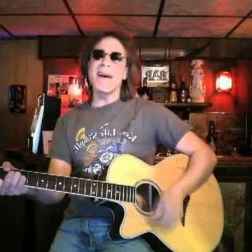
Mark Lauer

Mark Lauer

Mark Lauer

Mark Lauer
Mark Lauer
view source
Mark Lauer
view source
Mark Lauer
view source
Mark Lauer
view source
Mark Lauer
view source
Mark Lauer
view source
Mark M. Lauer
view source
Mark Lauer
view sourceGet Report for Mark C Lauer from Alameda, CA, age ~81

