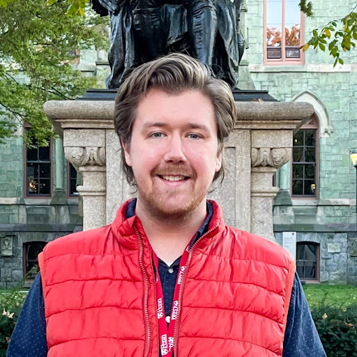
Michael Ray Sievers
age ~57
from Boise, ID
- Also known as:
-
- Michael R Sievers
- Michael A Sievers
- Mike R Sievers
- Jennifer Sievers
- Michael Sievens
- Micheal Sivers
Michael Sievers Phones & Addresses
- Boise, ID
- 30 Johns Blvd, Poughkeepsie, NY 12603 • 8454713135
- Havre, MT
- Frederick, CO
- East Fishkill, NY
- Raleigh, NC
- Salt Lake City, UT
- Sandy, UT
- 30 Johns Blvd, Poughkeepsie, NY 12603 • 3038273431
Work
-
Position:Retired
Education
-
Degree:Associate degree or higher
Us Patents
-
Focused Ion Beam Process For Removal Of Copper
view source -
US Patent:6730237, May 4, 2004
-
Filed:Jun 22, 2001
-
Appl. No.:09/887791
-
Inventors:Michael R. Sievers - Holmes NY
Steven B. Herschbein - Hopewell Junction NY
Aaron D. Shore - Poughkeepsie NY -
Assignee:International Business Machines Corporation - Armonk NY
-
International Classification:C23F 100
-
US Classification:216 62, 216 66, 216 78, 20412934
-
Abstract:A process for milling copper metal from a substrate having an exposed copper surface includes absorbing a halogen gas onto the exposed copper surface to generate reaction products of copper and the halogen gas; removing unreacted halogen gas from the surface; and directing a focused ion beam onto the surface to selectively remove a portion of the surface comprising the reaction products.
-
Metal Dry Etch Using Electronic Field
view source -
US Patent:6843893, Jan 18, 2005
-
Filed:Dec 12, 2002
-
Appl. No.:10/317679
-
Inventors:Steven B. Herschbein - Hopewell Junction NY, US
Herschel M. Marchman - Poughquag NY, US
Chad Rue - Poughkeepsie NY, US
Michael R. Sievers - Poughkeepsie NY, US -
Assignee:International Business Machines Corporation - Armonk NY
-
International Classification:C10B 100
H01L 21302 -
US Classification:204224M, 15634511, 15634539, 1563454
-
Abstract:A method and structure for an apparatus for removing metal from an integrated circuit structure is disclosed. A container holds an integrated circuit structure that has a metal portion. An electronic device connected to the container produces an electronic field proximate to a limited region of the metal portion. A first supply connected to the container supplies an oxidizing agent within the container. A solvent supply connected to the container supplies solvent to the limited region of the metal portion.
-
Dry Etch Process To Edit Copper Lines
view source -
US Patent:6900137, May 31, 2005
-
Filed:Mar 28, 2003
-
Appl. No.:10/249289
-
Inventors:Steven B. Herschbein - Hopewell Junction NY, US
Ville S. Kiiskinen - Newburgh NY, US
Chad Rue - Poughkeepsie NY, US
Carmelo F. Scrudato - Ossining NY, US
Michael R. Sievers - Poughkeepsie NY, US -
Assignee:International Business Machines Corporation - Armonk NY
-
International Classification:H01I021/302
-
US Classification:438712, 438705, 438714, 438717, 438725, 438734, 216 62, 216 66
-
Abstract:The present invention is directed to methods for editing copper features embedded within an organic body by exposing at least a portion of a top surface of the copper feature, forming a mill box there-over and then simultaneously milling both the copper feature and any organic material exposed through the mill box in a single step using an ion beam in combination with a XeFgas for a dwell time of at least 10 milliseconds. The invention dramatically increases the efficiency of Focused Ion Beam milling of copper features embedded in organic layers by milling these features in a gas-depleted environment at significantly increased dwell time while avoiding the problems of graphitization, destruction of the organic layer and metal redeposition.
-
Ion Detector For Ion Beam Applications
view source -
US Patent:7119333, Oct 10, 2006
-
Filed:Nov 10, 2004
-
Appl. No.:10/904438
-
Inventors:Steven B. Herschbein - Hopewell Junction NY, US
Narender Rana - Albany NY, US
Chad Rue - Poughkeepsie NY, US
Michael R. Sievers - Poughkeepsie NY, US -
Assignee:International Business Machines Corporation - Armonk NY
-
International Classification:G01N 23/225
H01J 37/00 -
US Classification:250309, 250397, 25049221
-
Abstract:Detection of weak ion currents scattered from a sample by an ion beam is improved by the use of a multiplier system in which a conversion electrode converts incident ions to a number of secondary electrons multiplied by a multiplication factor, the secondary electrons being attracted to an electron detector by an appropriate bias. In one version, the detector is a two stage system, in which the secondary electrons strike a scintillator that emits photons that are detected in a photon detector such as a photomultiplier or a CCD.
-
Non-Destructive In-Situ Elemental Profiling
view source -
US Patent:7256399, Aug 14, 2007
-
Filed:Apr 7, 2005
-
Appl. No.:10/907591
-
Inventors:Siddhartha Panda - Beacon NY, US
Michael R. Sievers - Poughkeepsie NY, US
Richard S. Wise - New Windsor NY, US -
Assignee:International Business Machines Corporation - Armonk NY
-
International Classification:G01N 23/227
-
US Classification:250305, 250307, 438 5, 438 10
-
Abstract:A non-destructive in-situ elemental profiling of a layer in a set of layers method and system are disclosed. In one embodiment, a first emission of a plurality of photoelectrons is caused from the layer to be elementally profiled. An elemental profile of the layer is determined based on the emission. In another embodiment, a second emission of a plurality of photoelectrons is also received from the layer, and an elemental profile is determined by comparison of the resulting signals. A process that is altering the layer can then be controlled “on-the-fly” to obtain a desired material composition. Since the method can be employed in-situ and is non-destructive, it reduces turn around time and lowers wafer consumption. The invention also records the composition of all processed wafers, hence, removing the conventional statistical sampling problem.
-
Gas Filled Reactive Atomic Force Microscope Probe
view source -
US Patent:7278300, Oct 9, 2007
-
Filed:Sep 29, 2005
-
Appl. No.:11/162958
-
Inventors:Michael R. Sievers - Poughkeepsie NY, US
Siddhartha Panda - Beacon NY, US
Richard Wise - New Windsor NY, US -
Assignee:International Business Machines Corporation - Armonk NY
-
International Classification:G01B 5/28
-
US Classification:73105
-
Abstract:An atomic force microscope (AFM) having a hollowed cantilever ending in a hollowed tip is described, wherein the end of the tip is immersed in a liquid. The AFM includes a gas source that provides and controls the flow of gas into the hollowed tip. The flow rate of the gas is regulated to form and sustain a static bubble at the end of the hollowed tip. The formation of the static bubble is verified optically. A gas control manifold allows an easy switch of gasses that are fed into the probe tip. The gas that is introduced acts like a chemically modified tip, and is selected to increase the deflection signal for the material of interest. The tip of the present invention is a highly versatile AFM tool that is easily adjusted to provide optimized imaging for a wide variety of materials, in contrast with standard AFMs that require a plethora of chemically modified tips to obtain equivalent results. Moreover, there is a much lower propensity for the tip to damage the sample or to be damaged from inadvertent contact with the surface of the sample.
-
Endpoint Detection For The Patterning Of Layered Materials
view source -
US Patent:7285775, Oct 23, 2007
-
Filed:Dec 2, 2004
-
Appl. No.:10/904883
-
Inventors:Michael R. Sievers - Poughkeepsie NY, US
Siddhartha Panda - Beacon NY, US
Richard Wise - New Windsor NY, US -
Assignee:International Business Machines Corporation - Armonk NY
-
International Classification:G01N 23/227
-
US Classification:250305, 250306, 250307, 378 89
-
Abstract:Photoelectron emissions are used to detect an endpoint of a thickness alteration of a topmost layer in a set of layers undergoing patterning. The set of layers are irradiated, which causes an emission of photoelectrons. Upon receipt of or absence of a photoelectron emission, patterning endpoint is detected.
-
Metal Oxide Field Effect Transistor With A Sharp Halo And A Method Of Forming The Transistor
view source -
US Patent:7384835, Jun 10, 2008
-
Filed:May 25, 2006
-
Appl. No.:11/420318
-
Inventors:Huajie Chen - Danbury CT, US
Judson R Holt - Wappingers Falls NY, US
Rangarajan Jagannathan - Hopewell Junction NY, US
Wesley C Natzle - New Paltz NY, US
Michael R Sievers - Poughkeepsie NY, US
Richard S Wise - Newburgh NY, US -
Assignee:International Business Machines Corporation - Armonk NY
-
International Classification:H01L 21/335
-
US Classification:438197, 257E21435
-
Abstract:Disclosed are embodiments of a MOSFET with defined halos that are bound to defined source/drain extensions and a method of forming the MOSFET. A semiconductor layer is etched to form recesses that undercut a gate dielectric layer. A low energy implant forms halos. Then, a COR pre-clean is performed and the recesses are filled by epitaxial deposition. The epi can be in-situ doped or subsequently implanted to form source/drain extensions. Alternatively, the etch is immediately followed by the COR pre-clean, which is followed by epitaxial deposition to fill the recesses. During the epitaxial deposition process, the deposited material is doped to form in-situ doped halos and, then, the dopant is switched to form in-situ doped source/drain extensions adjacent to the halos. Alternatively, after the in-situ doped halos are formed the deposition process is performed without dopants and an implant is used to form source/drain extensions.
Name / Title
Company / Classification
Phones & Addresses
18210 ST. CLAIR PROPERTIES, LLC
Resumes

Sr. Applications Engineer At Qcept Technologies
view sourcePosition:
Sr. Applications Engineer at Qcept Technologies
Location:
Greater New York City Area
Industry:
Semiconductors
Work:
Qcept Technologies - Fishkill, NY since Aug 2012
Sr. Applications Engineer
PDF Solutions - Poughkeepsie, NY Aug 2011 - Aug 2012
Sr. Consulting Engineer
Intellectual Ventures Apr 2010 - Dec 2011
Technical Consultant
Matheson Tri-Gas Oct 2008 - Apr 2010
Sr. Research Scientist
IBM 1999 - 2009
Etch Development Engineer
Sr. Applications Engineer
PDF Solutions - Poughkeepsie, NY Aug 2011 - Aug 2012
Sr. Consulting Engineer
Intellectual Ventures Apr 2010 - Dec 2011
Technical Consultant
Matheson Tri-Gas Oct 2008 - Apr 2010
Sr. Research Scientist
IBM 1999 - 2009
Etch Development Engineer
Education:
University of Utah 1992 - 2000
PhD, Chemistry Boise State University 1986 - 1990
BS, Chemistry
PhD, Chemistry Boise State University 1986 - 1990
BS, Chemistry

Michael Sievers
view sourceLocation:
United States

Michael Sievers
view sourceLocation:
United States
Googleplus

Michael Sievers
Lived:
Littleton, CO
Englewood, CO
Cheyenne, WY
Inverness, CO
Atlanta, GA
Sacramento, CA
Washington, DC
Alvin, TX
Bluefield, WV
Christiansburg, VA
El Paso, TX
Harlingen, TX
Hilliard, OH
Phoenix, AZ
Queens, NY
Thornton, CO
Tulsa, OK
Spartanburg, SC
Chicago, IL
New York City, NY
Gilbert, AZ
Monee, IL
New Braunfels, TX
Mt. Jackson, VA
Spokane, WA
Orange, NJ
Almelo, Netherlands
Madrid, Spain
Steeton, U.K.
Work:
Echostar Communications Corporation (1980-2008)
About:
DISH Network L.L.C., a subsidiary of DISH Network Corporation (NASDAQ:DISH), provides more than 14.3 million satellite TV customers, as of June 30, 2010, with the highest quality programming and techn...
Tagline:
Can't find Hopper, has anyone seen him?
Bragging Rights:
3rd Largest TV Provider in the US

Michael Sievers
Lived:
Denver, CO
Bloomington, IL
Chicago, IL
Peoria, IL
Bloomington, IL
Chicago, IL
Peoria, IL
Work:
DISH Network - Operations Analyst (2010)
DHL Global Forwarding - Ocean Import/Export Coordinator (2007-2008)
Affina - Product Specialist (2006-2006)
DHL Global Forwarding - Ocean Import/Export Coordinator (2007-2008)
Affina - Product Specialist (2006-2006)
Education:
Illinois Central College, Heartland Community College
About:
Oddball guy living the 'good' life and loving my Social Media job at DISH Network. Technophile. Geek. Nerd. Maybe. (So true).
Tagline:
Be Inspired
Bragging Rights:
Lost at one point over 200 pounds

Michael Sievers
Education:
South Jefferson High School

Michael Sievers

Michael Sievers

Michael Sievers

Michael Sievers

Michael Sievers
Youtube
Myspace

Michael Sievers
view sourcePlaxo

Michael Sievers
view sourceWalldorfGeschäftsführer at ZEIGMEHR WORKGROUP Geschäftsführer der ZEIGMEHR WORKGROUP Filmproduktion und Kreativagentur, am Puls der Zeit, neuen Trends stets auf der Spur, erfindungsreich, spontan... Geschäftsführer der ZEIGMEHR WORKGROUP Filmproduktion und Kreativagentur, am Puls der Zeit, neuen Trends stets auf der Spur, erfindungsreich, spontan, Projektleiter mit Zielblick, nimmermüde, schnell auf den Punkt, ideenreich und sehr flexibel, für die Kunden immer mit einem Trumpf im Ärmel und...
Flickr
Classmates

Michael Sievers
view sourceSchools:
Bridgewater-Raritan West High School Bridgewater NJ 1973-1977
Community:
Madilyn Leonard, Lawrence Trager, James Hann, Maureen Rose, Cindy Singer

Michael Sievers
view sourceSchools:
G.H. Whitcomb Elementary School Houston TX 1969-1975, Clear Lake Intermediate School Houston TX 1975-1978
Community:
Roland Kirkland, Laurie Coon

Michael Sievers
view sourceSchools:
Loyola College Preparatory School Shreveport LA 1992-1996
Community:
Rob Mitchell, Lisa Johnson, Robert Williams, Geralsine Alba, Joseph Joseph, Jim Beaux, Ellie Nowery, Todd Dixon, Patrick Ponce, Michele Gardner, Sarah Lindsey

Michael Sievers
view sourceSchools:
Bauxite High School Bauxite AR 1997-2001
Community:
Candias Haywood, Destini Vanmeter, Kellie Miller, Jake Myers, Christy Burnett, Brad Jackson, Amber Ragan, Michael Minnie, Jimmy Davis, Savahana Sowell

Michael Sievers, Fremont ...
view source
G.H. Whitcomb Elementary ...
view sourceGraduates:
Joyce Davis (1974-1976),
Patricia Northen (1968-1971),
Michael Sievers (1969-1975),
Tammy Case (1985-1986)
Patricia Northen (1968-1971),
Michael Sievers (1969-1975),
Tammy Case (1985-1986)

Fremont High School, Frem...
view sourceGraduates:
Michael Sievers (1962-1966),
Larry Stratman (1964-1968),
Todd Miles (1973-1977),
Kelcey Fox (1986-1990)
Larry Stratman (1964-1968),
Todd Miles (1973-1977),
Kelcey Fox (1986-1990)

Clear Lake Intermediate S...
view sourceGraduates:
Michael Sievers (1975-1978),
Edward Sachnik (1981-1984),
Dana Brittain (1986-1989),
Mariana Cunningham (1973-1974)
Edward Sachnik (1981-1984),
Dana Brittain (1986-1989),
Mariana Cunningham (1973-1974)

Michael Sievers
view source
Michael Sievers
view source
Michael Sievers
view source
Michael Sievers
view source
Michael Sievers
view source
Michael Sievers
view source
Michael Sievers
view source
Michael Sievers
view sourceGet Report for Michael Ray Sievers from Boise, ID, age ~57


