Nicholas E Webb
age ~46
from Milpitas, CA
- Also known as:
-
- Nicholas Edward Webb
- Nicholas Edwar Webb
- Phone and address:
- 1157 N Hillview Dr, Milpitas, CA 95035
Nicholas Webb Phones & Addresses
- 1157 N Hillview Dr, Milpitas, CA 95035
- Pollock Pines, CA
- Sacramento, CA
- Modesto, CA
- 851 3Rd St, Sauk Rapids, MN 56379 • 3206546354
- Madison, WI
- Fremont, CA
Specialities
Bankruptcy & Debt • Health Care • Employment & Labor • Social Security • Litigation • Personal Injury • Medical Malpractice
Resumes

Facilities Manager
view sourceWork:
Star Partner Enterprises Two, Llc
Facilities Manager
Facilities Manager
Education:
Brookside High School 2006
Skills:
Team Building
Microsoft Excel
Microsoft Office
Microsoft Word
Outlook
Editing
Project Management
Management
Project Planning
Troubleshooting
Inventory Management
Restaurants
Contract Management
Sales
Leadership Development
Microsoft Excel
Microsoft Office
Microsoft Word
Outlook
Editing
Project Management
Management
Project Planning
Troubleshooting
Inventory Management
Restaurants
Contract Management
Sales
Leadership Development

Nicholas Webb
view source
Nicholas Webb
view source
Nicholas Webb
view source
Nicholas Webb
view sourceLawyers & Attorneys

Nicholas Webb - Lawyer
view sourceSpecialties:
Bankruptcy & Debt
Health Care
Employment & Labor
Social Security
Litigation
Personal Injury
Medical Malpractice
Health Care
Employment & Labor
Social Security
Litigation
Personal Injury
Medical Malpractice
ISLN:
1000994712
Admitted:
2021
Isbn (Books And Publications)

Name / Title
Company / Classification
Phones & Addresses
OHIO RIVER LAND COMPANY I, LLC
OHIO RIVER LAND COMPANY II, LLC
OHIO RIVER LAND COMPANY III, LLC
OHIO RIVER LAND COMPANY IV, LLC
Manager
Frame Tech, LLC
Us Patents
-
Silicon Parts Having Reduced Metallic Impurity Concentration For Plasma Reaction Chambers
view source -
US Patent:6846726, Jan 25, 2005
-
Filed:Sep 20, 2002
-
Appl. No.:10/247722
-
Inventors:Daxing Ren - Pleasanton CA, US
Jerome S. Hubacek - Fremont CA, US
Nicholas E. Webb - Milpitas CA, US -
Assignee:Lam Research Corporation - Fremont CA
-
International Classification:H01L 2146
H01L 2178
H01L 21301 -
US Classification:438460, 438745, 438753
-
Abstract:Silicon parts of a semiconductor processing apparatus containing low levels of metal impurities that are highly mobile in silicon are provided. The silicon parts include, for example, rings, electrodes and electrode assemblies. The silicon parts can reduce metal contamination of wafers processed in plasma atmospheres.
-
Silicon Parts Having Reduced Metallic Impurity Concentration For Plasma Reaction Chambers
view source -
US Patent:7517803, Apr 14, 2009
-
Filed:Sep 28, 2004
-
Appl. No.:10/950656
-
Inventors:Daxing Ren - Pleasanton CA, US
Jerome S. Hubacek - Fremont CA, US
Nicholas E. Webb - Milpitas CA, US -
Assignee:Lam Research Corporation - Fremont CA
-
International Classification:H01L 21/302
-
US Classification:438710, 438706, 438719, 438729, 257E21218
-
Abstract:Silicon parts of a semiconductor processing apparatus containing low levels of metal impurities that are highly mobile in silicon are provided. The silicon parts include, for example, rings, electrodes and electrode assemblies. The silicon parts can reduce metal contamination of wafers processed in plasma atmospheres.
-
Etch Tool Process Indicator Method And Apparatus
view source -
US Patent:8492174, Jul 23, 2013
-
Filed:May 25, 2012
-
Appl. No.:13/481588
-
Inventors:Keren Jacobs Kanarik - Sunnyvale CA, US
Jorge Luque - Redwood City CA, US
Nicholas Webb - San Jose CA, US -
Assignee:Lam Research Corporation - Fremont CA
-
International Classification:G01R 31/26
-
US Classification:438 14, 257E21525
-
Abstract:A method for providing a process indicator for an etching chamber is provided. A wafer with a blanket etch layer is provided into the etching chamber. A blanket etch is performed on the blanket etch layer. A blanket deposition layer is deposited over the blanket etch layer after performing the blanket etch has been completed. A thickness of the blanket etch layer and a thickness of the blanket deposition layer is measured. The measured thicknesses are used to determine a process indicator.
-
Etch Tool Process Indicator Method And Apparatus
view source -
US Patent:8206996, Jun 26, 2012
-
Filed:Dec 15, 2009
-
Appl. No.:12/638697
-
Inventors:Keren Jacobs Kanarik - Sunnyvale CA, US
Jorge Luque - Redwood City CA, US
Nicholas Webb - San Jose CA, US -
Assignee:Lam Research Corporation - Fremont CA
-
International Classification:H01L 21/66
-
US Classification:438 14, 257E2153
-
Abstract:A method for providing a process indicator for an etching chamber is provided. A wafer with a blanket etch layer is provided into the etching chamber. A blanket etch is performed on the blanket etch layer. A blanket deposition layer is deposited over the blanket etch layer after performing the blanket etch has been completed. A thickness of the blanket etch layer and a thickness of the blanket deposition layer is measured. The measured thicknesses are used to determine a process indicator.
-
Haptic Feedback Device
view source -
US Patent:20120319827, Dec 20, 2012
-
Filed:Jun 17, 2011
-
Appl. No.:13/163532
-
Inventors:Aleksandar Pance - Saratoga CA, US
Nicholas U. Webb - Menlo Park CA, US
Sean A. Mayo - San Francisco CA, US -
Assignee:Apple Inc. - Cupertino CA
-
International Classification:H04B 3/36
-
US Classification:3404071
-
Abstract:A haptic feedback device configured to provide tactile or haptic feedback for an electronic device. The haptic device includes a platform operably secured to the electronic device to allow rotation about a center axis. An activating member is operably associated with the platform and configured to selectively cause the platform to rotate in a first direction. Also, the haptic feedback device includes a restoring member operably associated with the platform and configured to selectively return the platform to a first position after it has rotated for at least one of a select period of time or a select distance.
-
Electromagnetic Shielding Structures For Selectively Shielding Components On A Substrate
view source -
US Patent:20120320558, Dec 20, 2012
-
Filed:Jun 4, 2012
-
Appl. No.:13/488382
-
Inventors:James H. Foster - Palo Alto CA, US
James W. Bilanski - Palo Alto CA, US
Amir Salehi - San Jose CA, US
Ramamurthy Chandhrasekhar - Cupertino CA, US
Nicholas Unger Webb - Menlo Park CA, US -
International Classification:H05K 9/00
G01R 31/00
H05K 3/28
H05K 13/00
H05K 3/30
H05K 1/16
B23K 31/02 -
US Classification:361818, 174350, 174260, 32475016, 174388, 228164, 264319, 427 58, 156 84, 427125, 427554, 427 8, 29832, 29841, 29593
-
Abstract:Electronic components on a substrate may be shielded using electromagnetic shielding structures. Insulating materials may be used to provide structural support and to help prevent electrical shorting between conductive materials and the components. The shielding structures may include compartments formed using metal fences that surround selected components or by injection molding plastic. The shielding structures may be formed using metal foil wrapped over the components and the substrate. Electronic components may be tested using test posts or traces to identify components that are faulty. The test posts or traces may be deposited on the substrate and may be used to convey test signals between test equipment and the components. After successful testing, the test posts may be permanently shielded. Alternatively, temporary shielding structures may be used to allow testing of individual components before an electronic device is fully assembled.
-
Camera Assembly With Concave-Shaped Front Face
view source -
US Patent:20230108250, Apr 6, 2023
-
Filed:Dec 1, 2022
-
Appl. No.:18/060907
-
Inventors:- Mountain View CA, US
Kevin Edward Booth - Mountain View CA, US
Tyler Scott Wilson - San Francisco CA, US
Nicholas Webb - Menlo Park CA, US
Jason Evans Goulden - Los Gatos CA, US
William Dong - Redwood City CA, US
Jeffrey Law - San Francisco CA, US
Rochus Jacob - San Francisco CA, US
Adam Duckworth Mittleman - Redwood City CA, US
Oliver Mueller - San Francisco CA, US -
Assignee:Google LLC - Mountain View CA
-
International Classification:H04N 5/225
H04N 7/18
H04R 1/02
G02B 1/11
H04R 1/40
H04R 1/04
G03B 17/08
G02B 5/20
G08B 13/196
H04R 27/00
G03B 17/02
G03B 31/00
G03B 11/04 -
Abstract:The various implementations described herein include a video camera assembly that includes: (1) a housing; (2) an image sensor positioned within the housing and having a field of view corresponding to a scene in the smart home environment; and (3) a concave-shaped front face positioned in front of the image sensor such that light from the scene passes through the front face prior to entering the image sensor; where the front face includes: (a) an inner section corresponding to the image sensor; and (b) an outer section between the housing and the inner section, the outer section having a concave shape that extends from an outer periphery of the outer section to an inner periphery of the outer section; and where the concave shape extends around an entirety of the outer periphery.
-
Camera Assembly With Concave-Shaped Front Face
view source -
US Patent:20210344818, Nov 4, 2021
-
Filed:Jul 1, 2021
-
Appl. No.:17/365850
-
Inventors:- Mountain View CA, US
Kevin Edward Booth - Mountain View CA, US
Tyler Scott Wilson - San Francisco CA, US
Nicholas Webb - Menlo Park CA, US
Jason Evans Goulden - Los Gatos CA, US
William Dong - Redwood City CA, US
Jeffrey Law - San Francisco CA, US
Rochus Jacob - San Francisco CA, US
Adam Duckworth Mittleman - Redwood City CA, US
Oliver Mueller - San Francisco CA, US -
Assignee:Google LLC - Mountain View CA
-
International Classification:H04N 5/225
G02B 1/11
G08B 13/196
H04R 1/02
H04N 7/18
G03B 31/00
G03B 17/02
H04R 1/04
H04R 1/40
G02B 5/20
H04R 27/00
G03B 11/04
G03B 17/08 -
Abstract:The various implementations described herein include a video camera assembly that includes: (1) a housing; (2) an image sensor positioned within the housing and having a field of view corresponding to a scene in the smart home environment; and (3) a concave-shaped front face positioned in front of the image sensor such that light from the scene passes through the front face prior to entering the image sensor; where the front face includes: (a) an inner section corresponding to the image sensor; and (b) an outer section between the housing and the inner section, the outer section having a concave shape that extends from an outer periphery of the outer section to an inner periphery of the outer section; and where the concave shape extends around an entirety of the outer periphery.
Plaxo

Nicholas Webb
view sourceTokyoExecutive Investment Advisor at IFG Asia

Nicholas Webb
view sourceMarketing & Dealer Development at Brunswick Asia P...
Classmates

Nicholas Webb
view sourceSchools:
Lapel High School Lapel IN 1993-1997
Community:
Nancy Flaugher, Sherry Wolfe, Rachel Betz

Nicholas Webb
view sourceSchools:
Portage High School Portage IN 1996-2000
Community:
Edna Maturkanich, Rod Dennison, Kevin Durning

Nicholas Webb
view sourceSchools:
Lindstrom Elementary School Lakewood CA 1997-2001
Community:
Cyndee Barlass, Georgianne Glendenning, Calen Lybarger, Deborah Windisch, Barbara Dawson

Nicholas Webb
view sourceSchools:
Northridge High School Dayton OH 2005-2009
Community:
Bill Miller, Fred Coates

Nicholas Webb
view sourceSchools:
Abernathy Junior High School Abernathy TX 1999-2003
Community:
Cynthia Natal, Victoria Arreola, Angel Garcia, John Montgomery, Emily Petersen, Jennifer Garcia

Nicholas Webb
view sourceSchools:
Bourbon R-1 High School Bourbon MO 1992-1996
Community:
Scott Graddy, Stacy Parker, Jana Carrick, Lance Beckett, Neily Odam, William Greenlee, Daniel Whatley, Stacy Radford, Aimee Protte, Karl Campbell

Nicholas Webb
view sourceSchools:
Baden High School South San Francisco CA 1972-1976
Community:
Cindy Scarborough, Sylvia Pena, Pamela Zwerkowski, Chris Farron
Youtube
Myspace
Googleplus

Nicholas Webb
Education:
Simpson College - Political Science
Tagline:
I'm a wonderer and a wanderer.

Nicholas Webb
Work:
M on the Point - Bartedner

Nicholas Webb
Work:
Centa Left

Nicholas Webb
Tagline:
Real Estate Investments

Nicholas Webb
About:
Nicholas Webb is a prolific author with four books on the topic of innovation and customer experience, including “The Innovation Playbook,” “The Digital Innovation Playbook,” “The Innovation Superstar...
Tagline:
Speaker, author, inventor, CEO of Lassen Innovation
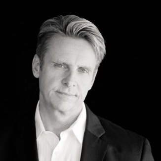
Nicholas Webb
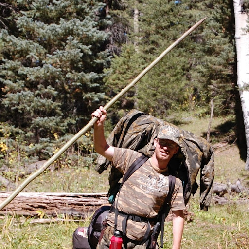
Nicholas Webb

Nicholas Webb

Nicholas Webb
view source
Nicholas Webb Sr.
view source
Nicholas Scott Webb
view source
Nicholas PalanceGod Webb
view source
Nicholas Webb
view source
Karl Nicholas Webb
view source
Nicholas Lyle Webb
view source
Nicholas Joe Webb
view sourceFlickr
Get Report for Nicholas E Webb from Milpitas, CA, age ~46


