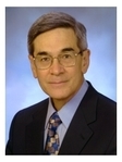
Richard L Elliott
age ~64
from Meridian, ID
- Also known as:
-
- Richard Lewis Elliott
- Richard L Elliot
- Rick Elliott
- Phone and address:
-
1833 Golfview Way, Meridian, ID 83642
2088552782
Richard Elliott Phones & Addresses
- 1833 Golfview Way, Meridian, ID 83642 • 2088552782
- 1923 Black Cat Rd, Meridian, ID 83642
- Boise, ID
- Navarre, FL
- Port Gamble, WA
Work
-
Company:San francisco cityApr 2013
-
Position:Senior epm consultant
Education
-
School / High School:CLEVELAND CHIROPRACTIC COLLEGE- Kansas City, MOAug 2006
-
Specialities:business
Resumes

Richard Elliott Lawrence, KS
view sourceWork:
San Francisco City
Apr 2013 to 2000
Senior EPM Consultant San Francisco City/County Government
San Francisco, CA
Dec 2012 to Apr 2013
Senior EPM Consultant/Senior SharePoint Architect Computer Science Corporation
Washington, DC
Sep 2012 to Nov 2012
Senior Architect TSA
Mar 2012 to Aug 2012
Senior SharePoint Architect/Consultant Lockheed Martin
Lexington, KY
Jul 2011 to Feb 2012
Senior Program Manager MRINetwork
Mar 2011 to Jul 2011
Senior Program Manager Data Solutions
May 2011 to May 2011
Senior Program Manager TEKSystems
Cedar Rapids, IA
Feb 2011 to Apr 2011
Senior Program Manager Covestic, Inc
Kirkland, WA
Sep 2010 to Feb 2011
Senior Program Manager Epicor Software Inc
Apr 2009 to Sep 2010
Principal consultant/strategist/PM on assignment Special Operations Forces
2010 to 2010
Principal consultant/strategist/PM on assignment Special Operations Forces
Kapolei, HI
2010 to 2010
Principal consultant/strategist/PM on assignment Cognizant
Jul 2008 to Apr 2009
Senior Program Manager Data Solutions
May 2001 to Jul 2008
Strategic Business Principal ePartners
Overland Park, KS
Aug 1994 to Apr 2001
Program Manager Miracle Computing
Lawrence, KS
Jan 1980 to Aug 1994
CEO/Strategic Business Principal
Education:
CLEVELAND CHIROPRACTIC COLLEGE
Kansas City, MO
Aug 2006 to Nov 2006
business Lawrence High School SharePoint Center of Excellence
design
Kansas City, MO
Aug 2006 to Nov 2006
business Lawrence High School SharePoint Center of Excellence
design
Medicine Doctors

Richard K. Elliott
view sourceSpecialties:
Gastroenterology
Work:
Affinity Clinical Gastroenterology
3722 Dressler Rd NW STE A, Canton, OH 44718
3304799000 (phone), 3304775805 (fax)
3722 Dressler Rd NW STE A, Canton, OH 44718
3304799000 (phone), 3304775805 (fax)
Education:
Medical School
Kansas City University of Medicine and Biosciences College of Osteopathic Medicine
Graduated: 1979
Kansas City University of Medicine and Biosciences College of Osteopathic Medicine
Graduated: 1979
Procedures:
Colonoscopy
Upper Gastrointestinal Endoscopy
Endoscopic Retrograde Cholangiopancreatography (ERCP)
Sigmoidoscopy
Upper Gastrointestinal Endoscopy
Endoscopic Retrograde Cholangiopancreatography (ERCP)
Sigmoidoscopy
Conditions:
Abdominal Hernia
Acute Pancreatitis
Acute Sinusitis
Anal Fissure
Anemia
Acute Pancreatitis
Acute Sinusitis
Anal Fissure
Anemia
Languages:
English
Description:
Dr. Elliott graduated from the Kansas City University of Medicine and Biosciences College of Osteopathic Medicine in 1979. He works in Canton, OH and specializes in Gastroenterology. Dr. Elliott is affiliated with Affinity Medical Center and Aultman Hospital.

Richard Lowen Elliott
view sourceSpecialties:
Ophthalmology
Pediatric Ophthalmology
Pediatric Ophthalmology
Education:
University of Southern California(1963)
License Records
Richard Schindler Elliott Md
License #:
4763 - Expired
Category:
Medicine
Issued Date:
May 22, 2002
Effective Date:
Oct 1, 2003
Expiration Date:
Oct 1, 2003
Type:
Backup PA Supervisor
Richard Schindler Elliott Md
License #:
4762 - Expired
Category:
Medicine
Issued Date:
May 22, 2002
Effective Date:
Oct 1, 2003
Expiration Date:
Oct 1, 2003
Type:
Backup PA Supervisor
Richard Schindler Elliott Md
License #:
4550 - Expired
Category:
Medicine
Issued Date:
Nov 7, 2001
Effective Date:
Oct 1, 2003
Expiration Date:
Oct 1, 2003
Type:
Backup PA Supervisor
Richard Schindler Elliott Md
License #:
4561 - Expired
Category:
Medicine
Issued Date:
Nov 7, 2001
Effective Date:
Oct 1, 2003
Expiration Date:
Oct 1, 2003
Type:
Backup PA Supervisor
Richard Schindler Elliott Md
License #:
4558 - Expired
Category:
Medicine
Issued Date:
Nov 7, 2001
Effective Date:
Oct 1, 2003
Expiration Date:
Oct 1, 2003
Type:
Backup PA Supervisor
Richard Schindler Elliott Md
License #:
4555 - Expired
Category:
Medicine
Issued Date:
Nov 7, 2001
Effective Date:
Oct 1, 2003
Expiration Date:
Oct 1, 2003
Type:
Backup PA Supervisor
Richard Schindler Elliott Md
License #:
3901 - Expired
Category:
Medicine
Issued Date:
Oct 20, 2000
Effective Date:
Nov 6, 2001
Expiration Date:
Oct 1, 2001
Type:
Backup PA Supervisor
Richard Schindler Elliott Md
License #:
3897 - Expired
Category:
Medicine
Issued Date:
Oct 20, 2000
Effective Date:
Oct 12, 2001
Expiration Date:
Oct 1, 2001
Type:
Backup PA Supervisor
Wikipedia

Richard Elliott Friedman
view sourceRichard Elliott Friedman is a biblical scholar and the Ann and Jay Davis Professor of Jewish Studies at the University of Georgia. He joined the faculty of the ...
Us Patents
-
Contact Integration Article
view source -
US Patent:6593657, Jul 15, 2003
-
Filed:Mar 3, 1997
-
Appl. No.:08/811124
-
Inventors:Richard L. Elliott - Meridian ID
Guy F. Hudson - Boise ID -
Assignee:Micron Technology, Inc. - Boise ID
-
International Classification:H01L 2348
-
US Classification:257765, 257767, 257764
-
Abstract:A method of making a contact plug and a metallization line structure is disclosed in which a substrate is provided with at least one contact hole within an insulation layer situated on a semiconductor substrate of a semiconductor wafer. A first metal layer is deposited upon the semiconductor wafer within the contact hole. A planarizing step isolates the first metal layer within the insulation layer in the form of a contact plug within the contact hole. A second metal layer is then deposited upon the semiconductor wafer over and upon the contact plug. Metallization lines are patterned and etched from the second metal layer. The contact hole may also be lined with a refractory metal nitride layer, with a refractory metal silicide interface being formed at the bottom of the contact hole as an interface between the contact plug and a silicon layer on the semiconductor substrate. Article qualities are achieved by the inventive method, including reduced interfacial resistance and its consequent faster signal speed for the structure, reduced metal creep where additional selected alloys are allowed to diffuse a selected quantity of preferred alloying elements from the first metal layer to the second metal layer, improved depth-of-focus requirements for patterning metallization lines, and resistance of electromigration in aluminum metallization lines.
-
Contact Integration Method
view source -
US Patent:6713384, Mar 30, 2004
-
Filed:Jan 16, 1998
-
Appl. No.:09/007949
-
Inventors:Richard L. Elliott - Meridian ID
Guy F. Hudson - Boise ID -
Assignee:Micron Technology, Inc. - Boise ID
-
International Classification:H01L 214763
-
US Classification:438625, 438627, 438660, 438688
-
Abstract:A method of making a contact plug and a metallization line structure is disclosed in which a substrate is provided with at least one contact hole within an insulation layer situated on a semiconductor substrate of a semiconductor wafer. A first metal layer is deposited upon the semiconductor wafer within the contact hole. A planarizing step isolates the first metal layer within the insulation layer in the form of a contact plug within the contact hole. A second metal layer is then deposited upon the semiconductor wafer over and upon the contact plug. Metallization lines are patterned and etched from the second metal layer. The contact hole may also be lined with a refractory metal nitride layer, with a refractory metal silicide interface being formed at the bottom of the contact hole as an interface between the contact plug and a silicon layer on the semiconductor substrate. Article qualities are achieved by the inventive method, including reduced interfacial resistance and its consequent faster signal speed for the structure, reduced metal creep where additional selected alloys are allowed to diffuse a selected quantity of preferred alloying elements from the first metal layer to the second metal layer, improved depth-of-focus requirements for patterning metallization lines, and resistance of electromigration in aluminum metallization lines.
-
Contact Integration Method
view source -
US Patent:7294570, Nov 13, 2007
-
Filed:Mar 29, 2004
-
Appl. No.:10/812117
-
Inventors:Richard L. Elliott - Meridian ID, US
Guy F. Hudson - Boise ID, US -
Assignee:Micron Technology, Inc. - Boise ID
-
International Classification:H01L 21/44
-
US Classification:438653, 438655, 438660, 438664, 257751, 257752, 257757, 257765, 257E21577, 257E21584, 257E21585
-
Abstract:A method of making a contact plug and a metallization line structure is disclosed in which a substrate is provided with at least one contact hole within an insulation layer situated on a semiconductor substrate of a semiconductor wafer. A first metal layer is deposited upon the semiconductor wafer within the contact hole. A planarizing step isolates the first metal layer within the insulation layer in the form of a contact plug within the contact hole. A second metal layer is then deposited upon the semiconductor wafer over and upon the contact plug. Metallization lines are patterned and etched from the second metal layer. The contact hole may also be lined with a refractory metal nitride layer, with a refractory metal silicide interface being formed at the bottom of the contact hole as an interface between the contact plug and a silicon layer on the semiconductor substrate. Article qualities are achieved by the inventive method, including reduced interfacial resistance and its consequent faster signal speed for the structure, reduced metal creep where additional selected alloys are allowed to diffuse a selected quantity of preferred alloying elements from the first metal layer to the second metal layer, improved depth-of-focus requirements for patterning metallization lines, and resistance of electromigration in aluminum metallization lines.
-
Ic Mechanical Planarization Process Incorporating Two Slurry Compositions For Faster Material Removal Times
view source -
US Patent:55408109, Jul 30, 1996
-
Filed:Jun 20, 1995
-
Appl. No.:8/493205
-
Inventors:Gurtej Sandhu - Boise ID
Richard L. Elliott - Boise ID
Trung T. Doan - Boise ID
Jody D. Larsen - Boise ID -
Assignee:Micron Technology Inc. - Boise ID
-
International Classification:H01L 2100
B24B 100 -
US Classification:1566361
-
Abstract:The present invention relates to integrated circuits (ICs) fabrication. Particularly, there is a cmp process which incorporates small quantities of two chemicals. The first chemical is the standard slurry mixtures, like water, aluminum-oxide and hydrogen-peroxide mixed into a slurry. The second chemical is a strong base chemical, like KOH, or potassium hydroxide. Moreover, the cmp process utilizes a system of closely regulating the timing of the two chemical process. Specifically, during a first time period, both chemicals are applied; thus increasing speed of the chemical removal of tungsten material. During a second time period, the KOH is removed, thus slowing down the chemical action and importantly achieving a greater degree of planerization than is capable by the two chemical first time period.
-
Trench/Hole Fill Processes For Semiconductor Fabrication
view source -
US Patent:59566124, Sep 21, 1999
-
Filed:Aug 9, 1996
-
Appl. No.:8/689535
-
Inventors:Richard L. Elliott - Meridian ID
John H. Givens - Meridian ID
Guy F. Hudson - Boise ID -
Assignee:MICRON Technology, Inc. - Boise ID
-
International Classification:H01L 21441
-
US Classification:438637
-
Abstract:A contact space filled with conductive material having good step coverage is disclosed. The contact space is formed in a dielectric layer with an upper surface. The contact space has sidewalls comprised of the dielectric layer and a bottom comprised of an underlying layer. The contact space is filled by first depositing a layer of an amorphous material such as TiAl. sub. 3 over the bottom and sidewalls of the contact space, then filling the contact space with a metallic fill material such as an aluminum-containing fill material. The amorphous material is chosen particularly to have low reactivity with the metallic fill material, so that mobility of the metallic fill material over the surface upon which it is deposited is facilitated.
-
Ic Mechanical Planarization Process Incorporating Two Slurry Compositions For Faster Material Removal Times
view source -
US Patent:59942240, Nov 30, 1999
-
Filed:Dec 17, 1997
-
Appl. No.:8/992399
-
Inventors:Gurtej S. Sandhu - Boise ID
Richard L. Elliott - Boise ID
Trung T. Doan - Boise ID
Jody D. Larsen - Boise ID -
Assignee:Micron Technology Inc. - Boise ID
-
International Classification:H01L 21304
-
US Classification:438692
-
Abstract:The present invention relates to integrated circuits (ICs) fabrication. Particularly, there is a cmp process which incorporates small quantities of two chemicals. The first chemical is the standard slurry mixtures, like water, aluminum-oxide and hydrogen-peroxide mixed into a slurry. The second chemical is a strong base chemical, like KOH, or potassium hydroxide. Moreover, the cmp process utilizes a system of closely regulating the timing of the two chemical process. Specifically, during a first time period, both chemicals are applied; thus increasing speed of the chemical removal of tungsten material. During a second time period, the KOH is removed, thus slowing down the chemical action and importantly achieving a greater degree of planerization than is capable by the two chemical first time period.
-
Spiral Grooved Polishing Pad For Chemical-Mechanical Planarization Of Semiconductor Wafers
view source -
US Patent:56905408, Nov 25, 1997
-
Filed:Feb 23, 1996
-
Appl. No.:8/606418
-
Inventors:Richard L. Elliott - Meridian ID
Michael A. Walker - Boise ID -
Assignee:Micron Technology, Inc. - Boise ID
-
International Classification:B24B 722
-
US Classification:451 41
-
Abstract:The present invention is a polishing pad for use in chemical-mechanical planarization of semiconductor wafers by placing a wafer against a polishing surface of the polishing pad while rotating the polishing pad about its center in the presence of a polishing slurry. The polishing surface has formed therein one or more grooves extending in a spiral inwardly from the periphery to the center of the polishing pad. As a result, slurry is transported inwardly toward the center or toward the periphery of the polishing pad depending upon the circumferential direction of the spiral relative to the direction of rotation of the polishing pad.
-
Method For Improved Bottom And Side Wall Coverage Of High Aspect Ratio Features
view source -
US Patent:59851031, Nov 16, 1999
-
Filed:Aug 14, 1997
-
Appl. No.:8/911151
-
Inventors:John H. Givens - Boise ID
Richard L. Elliott - Meridian ID -
Assignee:Micron Technology, Inc. - Boise ID
-
International Classification:C23C 1434
-
US Classification:20419212
-
Abstract:A method is disclosed for improved side wall and bottom coverage of high aspect ratio space situated upon a substrate in two (2) steps. A lining is formed on a side wall surface of the space that terminated at a bottom surface. An opening then remains to a void defined by the lining and the bottom surface. The void is filled with a material passing through the opening to the space. When sputtered, the lining can be formed by a less-collimated sputtered particle flux, and the void can be filled by a collimated sputtered particle flux. The lining can be formed by flux in a plasma formed from a first gas having a neutral to ion ratio, and the void can be filled by a flux in a plasma formed from a second gas having a neutral to ion ratio lower than that of the first. Also, the lining can be formed by a flux in a plasma formed from a first gas having an atomic mass, and the void can be filled by a flux in a plasma formed from a second gas having an atomic mass lower than that of the first. The lining can be formed by sputtering a target having a crystal structure not preferentially oriented to maximize collimation thereof, and the void can be filled with a flux from a target having a crystal structure preferentially oriented to maximize collimation thereof.
Lawyers & Attorneys

Richard W. Elliott, Bellevue WA - Lawyer
view sourceAddress:
Davis Wright Tremaine LLP
777 - 108Th Avenue Northeast, Bellevue, WA 98004
4256466140
777 - 108Th Avenue Northeast, Bellevue, WA 98004
4256466140
Licenses:
Washington - Active 1974
Education:
University of Washington School of Law
Degree - JD - Juris Doctor - Law
University of Washington
Degree - M.S. - Nuclear Engineering
Oregon State University
Degree - BA - Bachelor of Arts
Degree - JD - Juris Doctor - Law
University of Washington
Degree - M.S. - Nuclear Engineering
Oregon State University
Degree - BA - Bachelor of Arts
Specialties:
Appeals - 20%
Environmental / Natural Resources - 20%
Agriculture - 20%
Land Use / Zoning - 20%
Litigation - 20%
Environmental / Natural Resources - 20%
Agriculture - 20%
Land Use / Zoning - 20%
Litigation - 20%
Associations:
Asian Bar Association of Washington - Member
National Asian Pacific American Bar Association - Member
Washington State Bar Association - Member
National Asian Pacific American Bar Association - Member
Washington State Bar Association - Member

Richard David Elliott - Lawyer
view sourceAddress:
Davies Ward Phillips & Vineberg LLP
4168635506 (Office)
4168635506 (Office)
Licenses:
New York - Currently registered 2003
Education:
Osgoode Hall
Oxford University
Oxford University

Richard M Elliott - Lawyer
view sourceLicenses:
Dist. of Columbia - Active 1982

Richard Spencer Elliott - Lawyer
view sourceLicenses:
New York - Currently registered 1990
Education:
Columbia University School of Law

Richard Elliott - Lawyer
view sourceOffice:
Davenport Lyons
ISLN:
921635848
University:
Sheffield University, 1997; Sheffield University, 1997

Richard Elliott - Lawyer
view sourceOffice:
Richard J. Elliott
Specialties:
General Practice
Practice Law
Litigation
Practice Law
Litigation
ISLN:
907615727
Admitted:
1976
University:
California State University, Fullerton, B.A., 1969
Law School:
Baylor University, J.D., 1976

Richard Elliott - Lawyer
view sourceOffice:
Law Offices of Richard H. Elliott
Specialties:
Business Litigation
Elder Law
Ethics-Legal Malpractice
Investment Losses
Legal Malpractice
Litigation: Commercial
Litigation: Personal Injury
Products Liability
Securities Law
Trucking Litigation
Wrongful Death
Ethics & Professional Responsibility
Securities Offerings
Business
Arbitration
Ethics-Legal Malpractice
Administrative/Regulatory
International
ISLN:
907615741
Admitted:
1972
University:
Tulane University, B.A., 1969
Law School:
University of Texas, J.D., 1972
Name / Title
Company / Classification
Phones & Addresses
President
R. D. Elliott & Sons Roofing
1425508 Ontario Inc.. RD Elliott & Sons Roofing
Roofing Contractors
1425508 Ontario Inc.. RD Elliott & Sons Roofing
Roofing Contractors
2940 Quabin Road, R.R. # 3, Odessa, ON K0H 2HO
6133722837, 6133720388
6133722837, 6133720388
President
R. D. Elliott & Sons Roofing
Roofing Contractors
Roofing Contractors
6133722837, 6133720388
Incorporator
CREDIT BUREAU OF OXFORD
A. Elliott Investment Properties LLC
E & E OPERATING LLC
ELLIOTT DRIVE LLC
COACH, TRUCK & TRACTOR LLC
CTTK COMMUNICATION, LLC
Wikipedia References

Richard Elliott
Work:
Company:
Brigham Young University faculty
Position:Organist
Education:
Studied at:
The Catholic University of America • Curtis Institute of Music • Eastman School of Music
Academic degree:Professor
Skills & Activities:
Achieved status:
American Latter Day Saint
Activity:Convert to Mormonism

Richard Elliott (Organist)
Plaxo

Richard Elliott
view sourceMagna, UTClassifed Advertising at MediaOne of Utah Past: General Manager at The Employment Guide

Richard Elliott
view sourcePillerton Hersey UK

Richard Elliott
view sourceFinance Officer at Carers Centre Hull

Richard Elliott
view sourceSenior Business Analyst at CSC

Richard Elliott
view sourceToronto, ON, Canada

Richard Elliott
view sourceEuroclad
Googleplus

Richard Elliott
Work:
St. Andrew's On-the-Sound, Wilmington, NC - Rector (2002)
Holy Trinity, Clemson, SC - Curate (1979-1984)
St. Mark's, Venice, FL - Associate Rector (1984-1986)
St. Augustine's Chapel - Chaplain (1987-1994)
St. George's, Anderson, SC - Vicar (1995-2001)
Holy Trinity, Clemson, SC - Curate (1979-1984)
St. Mark's, Venice, FL - Associate Rector (1984-1986)
St. Augustine's Chapel - Chaplain (1987-1994)
St. George's, Anderson, SC - Vicar (1995-2001)
Education:
Centre College - History, Sewanee - School of Theology
Relationship:
Married
About:
Born in Lexington Kentucky. Married to Giles Singleton.
Bragging Rights:
Patriarch of the West

Richard Elliott
Lived:
Lynwood, CA
Yigo, Guam
Zaragoza, Spain
Rhineland-Palatinate, Germany
Pordenone, Italy
Crestview, Florida
Yigo, Guam
Zaragoza, Spain
Rhineland-Palatinate, Germany
Pordenone, Italy
Crestview, Florida
Work:
Lockheed Martin Aeronautics
Education:
Northwest Florida State College - Industrial Management, Kaplan University - Information Technology

Richard Elliott
Work:
Mohguhl Inc. - Owner (2008)
Education:
Wright State University - Musical Theater

Richard Elliott
Work:
The Bionetics Corporation (2007)
United States Air Force (1985-2005)
United States Air Force (1985-2005)
Tagline:
Don't touch my hat

Richard Elliott
Work:
Alcatel-Lucent
Education:
Bradford College

Richard Elliott
Education:
Northern Regional College

Richard Elliott
Education:
Samuel Clemens High School
Tagline:
Like to chill with friends and play ultimate frisbee and disc golf

Richard Elliott
Work:
UCD Inc. - Sales & Marketing Manager
About:
Sales and Marketing ManagerUCD Inc.February 2013 – Present (2 months)Kitchener, Canada AreaAt UCD Inc. we are commited to perfomance. Servicing the tri-city region and beyond for over 10 years we have...

Richard C Elliott
view source
John Richard Elliott
view source
Jo Richard Elliott
view source
Richard Elliott
view source
Richard Elliott
view source
Richard Elliott
view source
Richard Elliott Jr.
view source
Richard Elliott Turner
view sourceYoutube
Get Report for Richard L Elliott from Meridian, ID, age ~64


