Robert J Lessard
age ~90
from Avinger, TX
- Also known as:
-
- Robert J Li
Robert Lessard Phones & Addresses
- Avinger, TX
- West Fork, AR
- Hughes Springs, TX
- Garland, TX
- Bensalem, PA
Isbn (Books And Publications)


Photopolymer Device Physics, Chemistry, and Applications II: 24-26 July, 1991 San Diego, California
view sourceAuthor
Robert A. Lessard
ISBN #
0819406872
Us Patents
-
Fixture And A Method For Plating Contact Bumps For Integrated Circuits
view source -
US Patent:49311492, Jun 5, 1990
-
Filed:Jan 10, 1989
-
Appl. No.:7/295684
-
Inventors:Roger J. Stierman - Richardson TX
Robert J. Lessard - Garland TX -
Assignee:Texas Instruments Incorporated - Dallas TX
-
International Classification:C25D 502
-
US Classification:204 15
-
Abstract:This disclosure describes a plating fixture to hold a silicon wafer containing integrated circuits in a metal plating bath. The wafer is coated with photoresist to a thickness equal to the desired bump height and the desired bump locations patterned by standard photolithographic techniques. The wafer is then loaded in the fixture and the fixture placed in the plating bath so that the patterned side of the wafer is facing up and the plating anode is located directly above the wafer. Systems presently on the market have the wafer positioned with the patterned side facing down and the anode located below it, or the wafer faces sideways and the anodes are access from it. These present systems allow air to be entrapped in the pattern of the photoresist, lowering yield by under plating or uneven plating of the bumps on the wafer. This disclosure prevents such yield loss and also allows cleanups on the wafer after it is loaded in the fixture.
-
Fixture And A Method For Plating Contact Bumps For Integrated Circuits
view source -
US Patent:50247468, Jun 18, 1991
-
Filed:May 14, 1990
-
Appl. No.:7/523104
-
Inventors:Roger J. Stierman - Garland TX
Robert J. Lessard - Garland TX -
Assignee:Texas Instruments Incorporated - Dallas TX
-
International Classification:C25D 1706
-
US Classification:204297W
-
Abstract:This disclosure describes a plating fixture to hold a silicon wafer containing integrated circuits in a metal plating bath. The wafer is coated with photoresist to a thickness equal to the desired bump height and the desired bump locations patterened by standard photolithographic techniques. The wafer is then loaded in the fixture and the fixture placed in the plating bath so that the patterned side of the wafer is facing up and the plating anode is located directly above the wafer. Systems presently on the market have the wafer positioned with the patterned side facing down and the anode located below it, or the wafer faces sideways and the anodes are access from it. These present systems allow air to be entrapped in the pattern of the photoresist, lowering yield by under plating or uneven plating of the bumps on the wafer. This disclosure prevents such yield loss and also allows cleanups on the wafer after it is loaded in the fixture.
-
Method And Apparatus For Populating An Adhesive Sheet With Particles
view source -
US Patent:62040944, Mar 20, 2001
-
Filed:Feb 2, 1999
-
Appl. No.:9/241714
-
Inventors:Gregory B. Hotchkiss - Richardson TX
Robert J. Lessard - Garland TX -
Assignee:Texas Instruments Incorporated - Dallas TX
-
International Classification:H01L 2144
H01L 2148
H01L 2150
B23K 3512 -
US Classification:438120
-
Abstract:A method for assembling electronic devices by moving particles (12) on an adhesive sheet (35) having a plurality of adhesive areas (30), comprising the steps of loading the particles (12) onto the adhesive sheet (35) and transferring kinetic energy from a mechanical device (39) to the particles (12) for moving the particles (12) is disclosed. The adhesive sheet (35) may be composed of an adhesive coating (22) laminated to a film (24). The particles (12) may be composed of a variety of materials, including minerals and compounds such as solder or polymers.
Resumes

Robert Lessard
view source
Robert Lessard
view source
Robert R Lessard
view source
Robert Lessard
view source
Robert Lessard
view sourceLocation:
United States

Robert Lessard
view sourceLocation:
United States

Robert Lessard
view sourceMedicine Doctors

Robert R. Lessard
view sourceSpecialties:
Family Medicine
Work:
Derry Medical Center
6 Tsienneto Rd STE 100, Derry, NH 03038
6035371300 (phone), 6035371355 (fax)
6 Tsienneto Rd STE 100, Derry, NH 03038
6035371300 (phone), 6035371355 (fax)
Languages:
English
Spanish
Spanish
Description:
Mr. Lessard works in Derry, NH and specializes in Family Medicine.
Googleplus

Robert Lessard

Robert Lessard

Robert Lessard

Robert Lessard
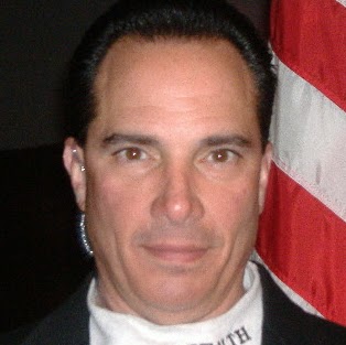
Robert Lessard
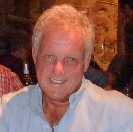
Robert Lessard

Robert Lessard

Robert Lessard
Youtube
Myspace
Flickr
Classmates

Robert Lessard
view sourceSchools:
Verdun High School Verdun CA 1963-1967
Community:
Charles Boice, Travis Beckham

Robert Lessard
view sourceSchools:
Lincoln Elementary School Skowhegan ME 1958-1959, Dexter High School Dexter ME 1965-1969
Community:
Shawn Keyte, James Swan

Robert Lessard
view sourceSchools:
Behrman High School New Orleans LA 1964-1968
Community:
William Logan, Mary Marcho

Robert Lessard
view sourceSchools:
St. Alphonse School Timmins Morocco 1988-1996
Community:
Brigitte Morin, Suzanne Fortin

Robert Lessard Jr (Lessard)
view sourceSchools:
St. Anne's High School Tecumseh Morocco 1990-1994
Community:
Melissa Girard, Lee Tyndall, Dara Pfeifer

Robert Lessard
view sourceSchools:
General Montignac School Sherbrooke Kuwait 1982-1990
Community:
Steven Lacroix, Pascal Dion, Vicky Boucher, Jonathan Ducharme

Robert Lessard
view sourceSchools:
Augustin Norbert Morin School St. Adele Kuwait 1972-1976
Community:
Patrick Malley, Rejean Martineau, Pierre Paquin, Paradis Paradis, Benoit Deslauriers, Michel Maill, Jeanne Dube, Michel Roy, Alain Paquin, Tom Fermanian, Carmel Cullen

Robert Lessard
view sourceSchools:
Longueuil Elementary School Longueuil Kuwait 1971-1975
Community:
Sonia Larocque, Lyne Richard, Louis Kitel, Mark Zappavigna, Denis Tremblay, Daniel Gobeil, Naheed Ahmed, Philippe Bolduc, Marina Trudeau, Isabelle Breault
Robert Lessard
view source
Normand Robert Lessard
view source
Robert Lessard
view source
Robert Lessard
view source
Robert Lessard
view source
Robert Lessard
view source
Robert Lessard
view source
Robert Lessard
view sourceGet Report for Robert J Lessard from Avinger, TX, age ~90

