Satish S Kulkarni
age ~54
from San Jose, CA
- Also known as:
-
- Satish Shankar Kulkarni
- Satish E Kulkarni
- Satish Kulkarni Mayuri
- Mayuri M Kulkarni
- Satish Shan
- Satish Kulkarini
- Satish Kumar
- Phone and address:
- 987 Wallace Dr, San Jose, CA 95120
Satish Kulkarni Phones & Addresses
- 987 Wallace Dr, San Jose, CA 95120
- Marietta, GA
- 5024 Barlow Dr, Round Rock, TX 78681 • 5122639913
- 104 Whitley Dr, Austin, TX 78738 • 5122639913
- 2117 Rodeo Cv, Austin, TX 78727 • 5122447064
- 3400 Ranch Road 620, Austin, TX 78738 • 5122639913
- Bee Cave, TX
- Grinnell, KS
- Edison, NJ
- Sunrise, FL
Us Patents
-
Reconfigurable Vector-Fft/Ifft, Vector-Multiplier/Divider
view source -
US Patent:7082451, Jul 25, 2006
-
Filed:Sep 9, 2002
-
Appl. No.:10/237465
-
Inventors:Satish S. Kulkarni - Austin TX, US
Brian T. Kelley - Austin TX, US -
Assignee:Freescale Semiconductor, Inc. - Austin TX
-
International Classification:G06F 15/00
-
US Classification:708404
-
Abstract:Systems and methods are described for providing a reconfigurable circuit having multiple distinct circuit configurations with respective distinct operating modes The circuit may be controllably configures to perform a fast Fourier transform function, a multiplier function, and a divider function. In one exemplary practical application of the invention, the fast Fourier transform function, multiplier function, and divider function may be used for signal demodulation, channel equalization and channel estimation for a WLAN IEEE 802. 11 system.
-
Communication Receiver
view source -
US Patent:7346098, Mar 18, 2008
-
Filed:Nov 25, 2003
-
Appl. No.:10/721950
-
Inventors:Weizhong Chen - Austin TX, US
Sekchin Chang - Austin TX, US
Satish S. Kulkarni - Austin TX, US -
Assignee:Freescale Semiconductor, Inc. - Austin TX
-
International Classification:H04B 1/00
-
US Classification:375150, 375136, 375147
-
Abstract:A timing and carrier error detector module () of a communication receiver (). The timing and carrier error detector module uses phase information of a correlated signal (e. g. a Barker de-spread signal) to generate a timing signal and carrier error signal. In one example, the phase information includes a phase error signal of the correlated signal. In one example, the timing and carrier error detector module calculates an indication of the variance of the phase error signal for a plurality of sample positions over a plurality of Barker symbol intervals. The timing signal is based upon the sample position having a minimum indication of a variance.
-
Communication Apparatus Having A Sim Interface Compatible With Radio Isolation
view source -
US Patent:7778674, Aug 17, 2010
-
Filed:Dec 29, 2004
-
Appl. No.:11/025673
-
Inventors:Frederick A. Rush - Austin TX, US
Satish S. Kulkarni - Austin TX, US -
Assignee:ST-Ericsson SA - Geneva
-
International Classification:H04M 1/00
-
US Classification:455574, 4555561, 455558, 713300, 710 13
-
Abstract:A communication apparatus including a radio frequency (RF) circuit coupled to a digital processing circuit and an interface circuit coupled to an authentication device. The RF circuit may be configured to operate on a radio frequency signal. A portion of the digital processing circuit may be disabled during an active mode of operation of the RF circuit. The interface circuit may be configured to buffer data communicated between the digital processing circuit and an authentication device during the active mode of operation of the RF circuit. In one embodiment, the interface circuit includes a memory and memory control logic to buffer data available for transmission to and/or received from the authentication device. In some embodiments, the digital processing circuit includes a processing unit configured to process authentication data received from the authentication device. In these and other embodiments, the authentication device may be a subscriber identity module (SIM).
-
Communication Apparatus Having A Standard Serial Communication Interface Compatible With Radio Isolation
view source -
US Patent:8019382, Sep 13, 2011
-
Filed:Dec 29, 2004
-
Appl. No.:11/025672
-
Inventors:Frederick A. Rush - Austin TX, US
Satish S. Kulkarni - Austin TX, US -
Assignee:ST-Ericsson SA - Plan-Les-Ouates
-
International Classification:H04M 1/00
-
US Classification:4555531, 455417, 455418, 4554261
-
Abstract:A communication apparatus including a digital processing circuit coupled to a radio frequency (RF) circuit and to a serial communications device. The serial communications device may be configured to buffer data communicated between the digital processing circuit and an external device. A portion of the serial communications device may be disabled during an active mode of operation of the RF circuit. The serial communications device may include a flow control logic circuit configured to control a data stream between the digital processing circuit and the external device while a portion of the serial communications device is disabled. In some embodiments, a portion of the digital processing circuit may be disabled during an active mode of operation of the RF circuit.
-
Method And Apparatus For Carrier Frequency Estimation And Correction For Gps
view source -
US Patent:20060058027, Mar 16, 2006
-
Filed:Sep 14, 2004
-
Appl. No.:10/940365
-
Inventors:Jing Fang - Austin TX, US
Satish Kulkarni - Austin TX, US -
Assignee:MOTOROLA, INC. - Schaumburg IL
-
International Classification:H04B 1/00
H04B 17/00
H04Q 7/20 -
US Classification:455434000, 455063100, 455067110
-
Abstract:A method and apparatus for frequency estimation useful in location determination utilizes a plurality of energy detectors to estimate the frequency associated with a peak energy value as determined by the energy detectors. An iterative process is implemented such that the frequency estimate corresponds to the Doppler frequency or carrier frequency error.
Medicine Doctors

Satish R. Kulkarni
view sourceSpecialties:
Psychiatry
Work:
Psychiatric Care Consultants
4905 Mexico Rd STE 300, Saint Peters, MO 63376
6369285109 (phone), 6364411081 (fax)
Center Pointe Hospital Psychiatry
4801 Weldon Spg Pkwy, Saint Charles, MO 63304
6364417300 (phone), 6364476001 (fax)
4905 Mexico Rd STE 300, Saint Peters, MO 63376
6369285109 (phone), 6364411081 (fax)
Center Pointe Hospital Psychiatry
4801 Weldon Spg Pkwy, Saint Charles, MO 63304
6364417300 (phone), 6364476001 (fax)
Education:
Medical School
J L Nehru Med Coll, R Gandhi Univ Hlth Sci, Belgaum, Karnataka, India
Graduated: 1974
J L Nehru Med Coll, R Gandhi Univ Hlth Sci, Belgaum, Karnataka, India
Graduated: 1974
Procedures:
Psychiatric Diagnosis or Evaluation
Psychiatric Therapeutic Procedures
Psychiatric Therapeutic Procedures
Conditions:
Bipolar Disorder
Depressive Disorders
Schizophrenia
Anxiety Dissociative and Somatoform Disorders
Anxiety Phobic Disorders
Depressive Disorders
Schizophrenia
Anxiety Dissociative and Somatoform Disorders
Anxiety Phobic Disorders
Languages:
English
Spanish
Spanish
Description:
Dr. Kulkarni graduated from the J L Nehru Med Coll, R Gandhi Univ Hlth Sci, Belgaum, Karnataka, India in 1974. He works in Saint Peters, MO and 1 other location and specializes in Psychiatry. Dr. Kulkarni is affiliated with Center Pointe Hospital.
Resumes

Director Of Energy Initiatives And Research Professor Of Engineering Science And Mechanics
view sourcePosition:
Director of Energy Initiatives & Research Prof of Eng Science and Mechanics at Virginia Tech
Location:
Arlington, Virginia
Industry:
Higher Education
Work:
Virginia Tech since Mar 2011
Director of Energy Initiatives & Research Prof of Eng Science and Mechanics
Virginia Tech 2011 - 2011
Director of Energy Initiatives
Georgetown Univ Apr 2009 - Sep 2010
Assoc Vice-President, New Initiatives & Partnerships
Director of Energy Initiatives & Research Prof of Eng Science and Mechanics
Virginia Tech 2011 - 2011
Director of Energy Initiatives
Georgetown Univ Apr 2009 - Sep 2010
Assoc Vice-President, New Initiatives & Partnerships

Director Of Engineering At Qualcomm
view sourcePosition:
Director of Engineering at Qualcomm
Location:
Bengaluru, Karnataka, India
Industry:
Wireless
Work:
Qualcomm - Bangalore, India since Jan 2012
Director of Engineering
ST-Ericsson - Bengaluru Area, India Mar 2010 - Dec 2011
Group Manager
ST-Ericsson - Austin, Texas, USA Feb 2009 - Feb 2010
Design Manager
ST-NXP Wireless - Austin, Texas, USA Aug 2008 - Feb 2009
Design Manager
NXP Semiconductors - Austin, Texas, USA Mar 2007 - Aug 2008
Design Manager
Education:
Oregon State University 1993 - 1994
MS, Electrical and Computer Engineering Indian Institute of Technology, Bombay 1988 - 1992
B.Tech., Electrical Engineering
MS, Electrical and Computer Engineering Indian Institute of Technology, Bombay 1988 - 1992
B.Tech., Electrical Engineering
Skills:
SoC
Mixed Signal
ASIC
Integrated Circuit Design
Low-power Design
Analog Circuit Design
PLL
RTL design
IC
Static Timing Analysis
Digital IC Design
CMOS
VLSI
Verilog
Semiconductors
Mixed Signal
ASIC
Integrated Circuit Design
Low-power Design
Analog Circuit Design
PLL
RTL design
IC
Static Timing Analysis
Digital IC Design
CMOS
VLSI
Verilog
Semiconductors

Satish Kulkarni
view sourceLocation:
United States

Director Of Engineering At Qualcomm
view sourcePosition:
Director of Engineering at Qualcomm
Location:
Bengaluru, Karnataka, India
Industry:
Wireless
Work:
Qualcomm - Bangalore, India since Jan 2012
Director of Engineering
ST-Ericsson - Bengaluru Area, India Mar 2010 - Dec 2011
Group Manager
ST-Ericsson - Austin, Texas, USA Feb 2009 - Feb 2010
Design Manager
ST-NXP Wireless - Austin, Texas, USA Aug 2008 - Feb 2009
Design Manager
NXP Semiconductors - Austin, Texas, USA Mar 2007 - Aug 2008
Design Manager
Director of Engineering
ST-Ericsson - Bengaluru Area, India Mar 2010 - Dec 2011
Group Manager
ST-Ericsson - Austin, Texas, USA Feb 2009 - Feb 2010
Design Manager
ST-NXP Wireless - Austin, Texas, USA Aug 2008 - Feb 2009
Design Manager
NXP Semiconductors - Austin, Texas, USA Mar 2007 - Aug 2008
Design Manager
Education:
Oregon State University 1993 - 1994
MS, Electrical and Computer Engineering Indian Institute of Technology, Bombay 1988 - 1992
B.Tech., Electrical Engineering
MS, Electrical and Computer Engineering Indian Institute of Technology, Bombay 1988 - 1992
B.Tech., Electrical Engineering
Skills:
SoC
Mixed Signal
ASIC
Integrated Circuit Design
Low-power Design
Analog Circuit Design
PLL
RTL design
IC
Static Timing Analysis
Digital IC Design
CMOS
VLSI
Verilog
Semiconductors
Mixed Signal
ASIC
Integrated Circuit Design
Low-power Design
Analog Circuit Design
PLL
RTL design
IC
Static Timing Analysis
Digital IC Design
CMOS
VLSI
Verilog
Semiconductors
Flickr
Youtube
Myspace

Satish B Kulkarni
view source
Satish Kulkarni
view source
Satish Kulkarni
view source
Satish Kulkarni
view source
Satish Kulkarni
view source
Satish Kulkarni
view source
Satish Kulkarni
view source
Satish Kulkarni
view sourceGoogleplus

Satish Kulkarni
Work:
TULIP GROUP OF COMPANIES - Manager Instruments Division
Education:
D.Y. PATIL COLLEGE OF ENGINEERING KOLHAPUR - B.E Electronics
About:
Staying in GOA. Professional in a Diagnostic Industry (TULIP DIAGNOSTICS P LTD)

Satish Kulkarni
Work:
GHPL - PLANT HEAD

Satish Kulkarni
Education:
C.l.boys high school
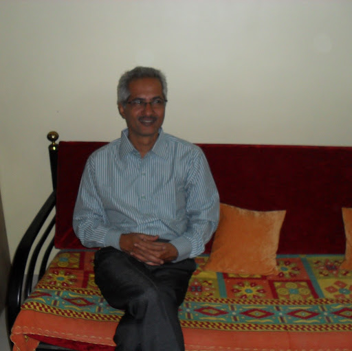
Satish Kulkarni

Satish Kulkarni

Satish Kulkarni

Satish Kulkarni

Satish Kulkarni
Plaxo

Satish Kulkarni
view sourceOwens Corning

Satish Kulkarni
view sourceAPS

Satish Kulkarni
view sourceOwens Corning
Get Report for Satish S Kulkarni from San Jose, CA, age ~54


