Steven A Lester
age ~78
from Acton, CA
- Also known as:
-
- Steven A Kallos
- Ste Lester
- Lester Ste
- Phone and address:
-
33105 Santiago Rd, Acton, CA 93510
6612695930
Steven Lester Phones & Addresses
- 33105 Santiago Rd, Acton, CA 93510 • 6612695930 • 6612700923
- 33105 Santiago Rd SPC 1, Acton, CA 93510 • 6612695930
- San Jose, CA
- Pineville, AR
- Las Vegas, NV
- San Bernardino, CA
- Paso Robles, CA
- Eureka, CA
- Los Angeles, CA
- Palmdale, CA
Work
-
Company:Pasadena area community college district
-
Address:1570 E Colorado Blvd, Pasadena, CA 91106
-
Phones:6265857716
-
Position:Senior college safety officer
-
Industries:Junior Colleges and Technical Institutes
Resumes
Lawyers & Attorneys
Medicine Doctors

Steven J. Lester
view sourceSpecialties:
Cardiovascular Disease
Work:
Mayo Clinic
13400 E Shea Blvd, Scottsdale, AZ 85259
4803018000 (phone), 4803422544 (fax)
Mayo ClinicMayo Clinic Hospital Arizona
5777 E Mayo Blvd, Phoenix, AZ 85054
4803018000 (phone), 4803423475 (fax)
13400 E Shea Blvd, Scottsdale, AZ 85259
4803018000 (phone), 4803422544 (fax)
Mayo ClinicMayo Clinic Hospital Arizona
5777 E Mayo Blvd, Phoenix, AZ 85054
4803018000 (phone), 4803423475 (fax)
Education:
Medical School
Univ of Toronto, Fac of Med, Toronto, Ont, Canada
Graduated: 1991
Univ of Toronto, Fac of Med, Toronto, Ont, Canada
Graduated: 1991
Procedures:
Bone Marrow Biopsy
Cardioversion
Cardiac Stress Test
Echocardiogram
Electrocardiogram (EKG or ECG)
Nutrition Therapy
Pulmonary Function Tests
Cardioversion
Cardiac Stress Test
Echocardiogram
Electrocardiogram (EKG or ECG)
Nutrition Therapy
Pulmonary Function Tests
Conditions:
Atrial Fibrillation and Atrial Flutter
Cardiomyopathy
Conduction Disorders
Disorders of Lipoid Metabolism
Heart Failure
Cardiomyopathy
Conduction Disorders
Disorders of Lipoid Metabolism
Heart Failure
Languages:
English
Spanish
Spanish
Description:
Dr. Lester graduated from the Univ of Toronto, Fac of Med, Toronto, Ont, Canada in 1991. He works in Scottsdale, AZ and 1 other location and specializes in Cardiovascular Disease. Dr. Lester is affiliated with Mayo Clinic Hospital.

Steven E. Lester
view sourceSpecialties:
General Surgery
Work:
Kaiser Permanente Medical GroupKaiser Permanente Westside Hospital Surgery
2875 NW Stucki Ave, Hillsboro, OR 97124
5035715780 (phone), 9713103926 (fax)
2875 NW Stucki Ave, Hillsboro, OR 97124
5035715780 (phone), 9713103926 (fax)
Education:
Medical School
University of Washington SOM
Graduated: 1986
University of Washington SOM
Graduated: 1986
Procedures:
Breast Reconstruction
Breast Reduction
Mastectomy
Thoracoscopy
Breast Biopsy
Colonoscopy
Endoscopic Retrograde Cholangiopancreatography (ERCP)
Hemorrhoid Procedures
Hernia Repair
Laparoscopic Gallbladder Removal
Pilonidal Cyst Excision
Upper Gastrointestinal Endoscopy
Breast Reduction
Mastectomy
Thoracoscopy
Breast Biopsy
Colonoscopy
Endoscopic Retrograde Cholangiopancreatography (ERCP)
Hemorrhoid Procedures
Hernia Repair
Laparoscopic Gallbladder Removal
Pilonidal Cyst Excision
Upper Gastrointestinal Endoscopy
Conditions:
Abdominal Hernia
Cholelethiasis or Cholecystitis
Inguinal Hernia
Malignant Neoplasm of Female Breast
Cholelethiasis or Cholecystitis
Inguinal Hernia
Malignant Neoplasm of Female Breast
Languages:
English
Description:
Dr. Lester graduated from the University of Washington SOM in 1986. He works in Hillsboro, OR and specializes in General Surgery. Dr. Lester is affiliated with Kaiser Sunnyside Medical Center and Providence Saint Vincent Medical Center.

Steven G. Lester
view sourceSpecialties:
Radiation Oncology
Work:
Radiation Oncology Consultants
2200 W 1 St, Sanford, FL 32771
4073213040 (phone), 4073213041 (fax)
Radiation Oncology Consultants
52 W Gore St, Orlando, FL 32806
4072032700 (phone), 8552354945 (fax)
2200 W 1 St, Sanford, FL 32771
4073213040 (phone), 4073213041 (fax)
Radiation Oncology Consultants
52 W Gore St, Orlando, FL 32806
4072032700 (phone), 8552354945 (fax)
Education:
Medical School
Louisiana State University School of Medicine at Shreveport
Graduated: 1982
Louisiana State University School of Medicine at Shreveport
Graduated: 1982
Languages:
English
Description:
Dr. Lester graduated from the Louisiana State University School of Medicine at Shreveport in 1982. He works in Sanford, FL and 1 other location and specializes in Radiation Oncology. Dr. Lester is affiliated with Central Florida Regional Hospital and Orlando Regional Medical Center.
Name / Title
Company / Classification
Phones & Addresses
Senior College Safety Officer
Pasadena Area Community College District
Junior Colleges and Technical Institutes
Junior Colleges and Technical Institutes
1570 E Colorado Blvd, Pasadena, CA 91106
Manager
S.D.O.G. Holdings, LLC
Sea View Estates LLC
Real Estate · Business Services at Non-Commercial Site · Nonclassifiable Establishments
Real Estate · Business Services at Non-Commercial Site · Nonclassifiable Establishments
33105 Santiago Rd, Acton, CA 93510
Rancho Paso I LLC
Real Estate · General Animal Farm
Real Estate · General Animal Farm
33105 Santiago Rd, Acton, CA 93510
Manager
Nnn Reno Trademark 2, LLC
33105 Santiago Rd, Acton, CA 93510
President, President, Secretary, Treasurer
KINGSPORT VALLEY, INC
33105-118 Santiago Rd, Acton, CA 93510
33105 Santiago Rd, Acton, CA 93510
33105 Santiago Rd, Acton, CA 93510
Sea View Estates L.P
33105 Santiago Rd, Acton, CA 93510
Ranco Paso L.P
33105 Santiago Rd, Acton, CA 93510
Us Patents
-
Highly Reflective Ohmic Contacts To Iii-Nitride Flip-Chip Leds
view source -
US Patent:6573537, Jun 3, 2003
-
Filed:Mar 29, 2001
-
Appl. No.:09/821684
-
Inventors:Daniel A. Steigerwald - Cupertino CA
Steven D. Lester - Palo Alto CA -
Assignee:Lumileds Lighting, U.S., LLC - San Jose CA
-
International Classification:H01L 3300
-
US Classification:257103, 257 79, 257 91, 257 94, 257 96, 257 98, 257 99
-
Abstract:An inverted III-nitride light-emitting device (LED) with highly reflective ohmic contacts includes n- and p-electrode metallizations that are opaque, highly reflective, and provide excellent current spreading. The n- and p-electrodes each absorb less than 25% of incident light per pass at the peak emission wavelength of the LED active region.
-
Monolithic Multi-Wavelength Vertical-Cavity Surface Emitting Laser Array And Method Of Manufacture Therefor
view source -
US Patent:6806110, Oct 19, 2004
-
Filed:May 16, 2002
-
Appl. No.:10/151646
-
Inventors:Steven D. Lester - Palo Alto CA
Virginia M. Robbins - Los Gatos CA
Jeffrey N. Miller - Los Altos Hills CA -
Assignee:Agilent Technologies, Inc. - Palo Alto CA
-
International Classification:H01L 2100
-
US Classification:438 28, 438 34
-
Abstract:A monolithic array of vertical cavity lasers with different emission wavelengths on a single wafer, and method of manufacture therefor, is provided. A first reflector is over the semiconductor substrate with a photoactive semiconductor layer. A reflector support defines first and second air gaps with the photoactive semiconductor layer. The second and third air gaps are made to be different from each other by geometric differences in the reflector support structure. Second and third reflectors are formed over the reflector support whereby a first laser is formed by the first reflector, the photoactive semiconductor structure, the first air gap, and the second reflector and whereby a second laser is formed by the first reflector, the photoactive semiconductor structure, the second air gap, and the third reflector. The emission wavelengths of the first and second lasers are different because of the different sizes of the first and second air gaps.
-
Fixed Wavelength Vertical Cavity Optical Devices And Method Of Manufacture Therefor
view source -
US Patent:6953702, Oct 11, 2005
-
Filed:May 16, 2002
-
Appl. No.:10/151631
-
Inventors:Jeffrey N. Miller - Los Altos Hills CA, US
Virginia M. Robbins - Los Gatos CA, US
Steven D. Lester - Palo Alto CA, US -
Assignee:Agilent Technologies, Inc. - Palo Alto CA
-
International Classification:H01L021/20
-
US Classification:438 22, 438 35
-
Abstract:Vertical cavity optical devices, and a method of manufacturing therefor, are provided where the method includes partially forming a first vertical cavity optical device on a wafer, adjusting the lasing wavelength of the first vertical cavity optical device, and fixing the lasing wavelength of the first vertical cavity optical device to complete the forming thereof.
-
Method And Structure For Improved Led Light Output
view source -
US Patent:7095052, Aug 22, 2006
-
Filed:Oct 22, 2004
-
Appl. No.:10/971380
-
Inventors:Steven D. Lester - Palo Alto CA, US
-
Assignee:Avago Technologies ECBU IP (Singapore) Pte. Ltd. - Singapore
-
International Classification:H01L 27/15
-
US Classification:257 79, 257 88, 257 89, 257 90, 257 94
-
Abstract:The efficiency of LEDs is increased by incorporating multiple active in series separated by tunnel junction diodes. This also allows the LEDs to operate at longer wavelengths.
-
Gallium Nitride Device Substrate Containing A Lattice Parameter Altering Element
view source -
US Patent:7273798, Sep 25, 2007
-
Filed:Aug 1, 2005
-
Appl. No.:11/194237
-
Inventors:Steven D. Lester - Palo Alto CA, US
Virginia M. Robbins - Los Gatos CA, US
Scott W. Corzine - Sunnyvale CA, US -
Assignee:Avago Technologies ECBU IP (Singapore) Pte. Ltd. - Singapore
-
International Classification:H01L 21/301
H01L 21/461 -
US Classification:438458, 438455
-
Abstract:A gallium nitride device substrate comprises a layer of gallium nitride containing an additional lattice parameter altering element located over a substitute substrate.
-
Structures For Reducing Operating Voltage In A Semiconductor Device
view source -
US Patent:7473941, Jan 6, 2009
-
Filed:Aug 15, 2005
-
Appl. No.:11/203917
-
Inventors:Virginia M. Robbins - Los Gatos CA, US
Steven D. Lester - Palo Alto CA, US
Jeffrey N. Miller - Los Altos Hills CA, US
David P. Bour - Cupertino CA, US -
Assignee:Avago Technologies ECBU IP (Singapore) Pte. Ltd. - Singapore
-
International Classification:H01L 33/00
-
US Classification:257102, 257104
-
Abstract:A light-emitting device comprises an active region configured to generate light in response to injected charge, and an n-type material layer and a p-type material layer, wherein at least one of the n-type material layer and the p-type material layer is doped with at least two dopants, at least one of the dopants having an ionization energy higher than the ionization energy level of the other dopant.
-
Ohmic Contact On P-Type Gan
view source -
US Patent:7495314, Feb 24, 2009
-
Filed:Sep 26, 2005
-
Appl. No.:11/234993
-
Inventors:Jeffrey N. Miller - Los Altos Hills CA, US
David P. Bour - Cupertino CA, US
Virginia M. Robbins - Los Gatos CA, US
Steven D. Lester - Palo Alto CA, US -
Assignee:Avago Technologies ECBU IP (Singapore) Pte. Ltd. - Singapore
-
International Classification:H01L 29/22
-
US Classification:257614, 257744, 257741, 257750, 257 78, 257191, 438 37
-
Abstract:An ohmic contact in accordance with the invention includes a layer of p-type GaN-based material. A first layer of a group II-VI compound semiconductor is located adjacent to the layer of p-type GaN-based material. The ohmic contact further includes a metal layer that provides metal contact. A second layer of a different II-VI compound semiconductor is located adjacent to the metal layer.
-
Led Electrode
view source -
US Patent:7573074, Aug 11, 2009
-
Filed:May 19, 2006
-
Appl. No.:11/437570
-
Inventors:Frank T. Shum - Sunnyvale CA, US
William W. So - Sunnyvale CA, US
Steven D. Lester - Sunnyvale CA, US -
Assignee:Bridgelux, Inc. - Sunnyvale CA
-
International Classification:H01L 33/00
H01L 29/22 -
US Classification:257 99, 257 88, 257 98, 257103, 257E33068, 257E27121, 372 4501, 372 45011, 372 501, 438 25, 438 35
-
Abstract:An electrode structure is disclosed for enhancing the brightness and/or efficiency of an LED. The electrode structure can have a metal electrode and an optically transmissive thick dielectric material formed intermediate the electrode and a light emitting semiconductor material. The electrode and the thick dielectric cooperate to reflect light from the semiconductor material back into the semiconductor so as to enhance the likelihood of the light ultimately being transmitted from the semiconductor material. Such LED can have enhanced utility and can be suitable for uses such as general illumination.
Youtube
Myspace
Flickr
Plaxo

Steven Lester
view sourceEast BaySteven Lester Co Past: Partner at Sonic Marketing "The High End AV Rep for the residential market focusing on benchmark brands and technologies. Demos, sales training, mentoring and motivation with the long... "The High End AV Rep for the residential market focusing on benchmark brands and technologies. Demos, sales training, mentoring and motivation with the long term success for brand and dealer as sole purpose.
Classmates

Steven Lester
view sourceSchools:
Mableton High School Mableton GA 1999-2003
Community:
Kemal Boggs

Steven Lester
view sourceSchools:
Washington Elementary School Burbank CA 1956-1963
Community:
Tom Evans, Linda Holtz

Steven Lester
view sourceSchools:
Nielsen Elementary School Dublin CA 1979-1983
Community:
James Castillo, Jennifer Ross, Robyn Hardman

Steven Lester
view sourceSchools:
Garden High School Oakwood VA 1991-1995
Community:
Keen Stacy, Deborah Noe, Sudale Barnett

Steven Lester
view sourceSchools:
Downingtown High School Downingtown PA 1969-1973
Community:
Charlene Barton

Steven Lester
view sourceSchools:
La Cueva High School Albuquerque NM 2004-2008
Community:
Betty Edelman, Kody Simmons

Steven Lester
view sourceSchools:
Leonard High School Leonard TX 1997-2001
Community:
Jerry Watts, Judy Casteel, Patrice Harris, Art Ragland

Steven Lester
view sourceSchools:
Millburn West School Lindenhurst IL 2002-2006
Community:
Noah Rose, Terri Clay, Cindy Longo, Emily Denman, Sarah Lucas, Alexis Koth, Michael Thorne, Jessica Schmitt, Tim Presley, Darien Mccullough, Sabrina Kilar
Googleplus
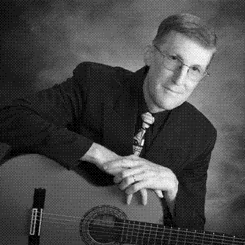
Steven Lester
Work:
Lake Placid Music - Sole Proprietor
Steven Lester

Steven Lester

Steven Lester

Steven Lester
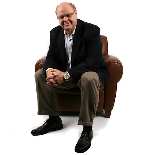
Steven Lester

Steven Lester
Education:
Olathe North High
Tagline:
I enjoy time with family, water skiing, horse back riding and volunteer as a ham radio operator.
Bragging Rights:
Made it through High School and some College

Steven Lester

Steven Lester
view source
Steven D. Lester
view source
Steven Lester
view source
Steven Lester
view source
Steven Lester
view source
Steven Lester
view source
Steven Lester Gamba
view source
Steven Lester
view sourceGet Report for Steven A Lester from Acton, CA, age ~78


