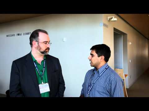
Vikas B Gupta
age ~45
from Holly Springs, NC
- Also known as:
-
- Gupta Vikas
Vikas Gupta Phones & Addresses
- Holly Springs, NC
- Morrisville, NC
- Sunnyvale, CA
Name / Title
Company / Classification
Phones & Addresses
Branch Manager
Arrow Truck Sales
Truck Dealers
Truck Dealers
1285 Shawson Drive, Mississauga, ON L4W 1C4
9055643411, 9055643419
9055643411, 9055643419
Branch Manager
Arrow Truck Sales
Truck Dealers
Truck Dealers
9055643411, 9055643419
President
Wonder Workshop Inc
Computer Programming Svc Mfg Games/Toys Whol Toys/Hobby Goods Ret Hobbies/Toys/Games · Custom Computer Programing · Custom Computer Programming Services, Nsk · Telephone Communication, Except Radio
Computer Programming Svc Mfg Games/Toys Whol Toys/Hobby Goods Ret Hobbies/Toys/Games · Custom Computer Programing · Custom Computer Programming Services, Nsk · Telephone Communication, Except Radio
550 E Weddell Dr, Sunnyvale, CA 94089
2121 S El Camino Real, San Mateo, CA 94403
6502421499
2121 S El Camino Real, San Mateo, CA 94403
6502421499
President
IPTE VENTURES INC
Business Services
Business Services
829 S Knikerbocker Dr, Sunnyvale, CA 94087
829 S Knickerbocker Dr, Sunnyvale, CA 94087
829 S Knickerbocker Dr, Sunnyvale, CA 94087
President
AKSHIT INCORPORATION
1700 Halford Ave #125, Santa Clara, CA 95051
Managing
Seven River Investment, LLC
Real Estate Selling Property for Others
Real Estate Selling Property for Others
3766 Pinewood Pl, Santa Clara, CA 95054
Resumes

Vikas Gupta
view sourceLocation:
Naperville, Illinois
Industry:
Information Technology and Services
Skills:
MatrixOne
Google Docs
Google Apps
.NET
SAP
Java Enterprise Edition
Enterprise Software
EAI
SOA
Business Analysis
Requirements Analysis
Integration
SaaS
Professional Services
ERP
Cloud Computing
Vendor Management
Weblogic
SAP Netweaver
Google Docs
Google Apps
.NET
SAP
Java Enterprise Edition
Enterprise Software
EAI
SOA
Business Analysis
Requirements Analysis
Integration
SaaS
Professional Services
ERP
Cloud Computing
Vendor Management
Weblogic
SAP Netweaver

Project Lead, Hcl America Inc
view sourcePosition:
Project Lead at HCL Technologies
Location:
Hillsboro, Oregon
Industry:
Consumer Electronics
Work:
HCL Technologies since Oct 2009
Project Lead
Intel Corporation - Chandler Aug 2011 - Jun 2013
Audio DSP Consultant(Contractual Position)
Zoran - Sunnyvale,CA Nov 2009 - Jul 2011
Audio DSP Consultant(Contractual Position)
HCL Technologies - Noida Area, India Oct 2006 - Oct 2009
Lead Engg
Sony - Bengaluru Area, India(Formerly know as Bangalore) Feb 2005 - Oct 2006
Junior Staff Engg.
Education:
Rajasthan University 2000 - 2004
B.E, CSE Board of Secondary Education,Rajasthan 1998 - 1999
High School, Mathematics and Computer Science
B.E, CSE Board of Secondary Education,Rajasthan 1998 - 1999
High School, Mathematics and Computer Science
Skills:
C
Shell Scripting
C++
MIPS
MPEG
ThreadX
Embedded Systems
ARM
Firmware
RTOS
Debugging
Device Drivers
Set Top Box
IPTV
HDTV
Audio Post Production
Audio Processing
Digital Signal Processing
Linux
Linux Kernel
Ubuntu
Dolby
AAC
MP3
MPEG-4
MPEG2
ATSC
DVB-T
G729
IEC 61937
IEC 60958
Clocks
Embedded Software
Embedded Linux
Digital TV
SoC
DVB
H.264
Digital Signal Processors
Algorithms
Software Development
ClearCase
Unix
Consumer Electronics
Perforce
Multithreading
Middleware
Agile Methodologies
Processors
EDA
Certifications:
Linux Kernel Certification

Vikas Gupta
view sourceLocation:
United States

Global Delivery Manager At Cognizant Technology Solutions
view sourcePosition:
Senior Delivery Manager at Cognizant Technology Solutions
Location:
Chester Springs, Pennsylvania
Industry:
Information Services
Work:
Cognizant Technology Solutions - Wilmington, DE since Aug 2004
Senior Delivery Manager
Cognizant Technology Solutions Aug 2004 - Jul 2008
Portfolio Manager
Senior Delivery Manager
Cognizant Technology Solutions Aug 2004 - Jul 2008
Portfolio Manager
Education:
Barkatullah Vishwavidyalaya
B E
B E
Interests:
Mobile Technologies, camping, hiking
Honor & Awards:
Process Pioneer Award, Innovation Award

Vikas Gupta
view sourceLocation:
United States

Business Developer At Shrey Infotech
view sourcePosition:
business developer at shrey infotech
Location:
United States
Industry:
Staffing and Recruiting
Work:
shrey infotech
business developer
business developer
Education:
Kurukshetra University 2002 - 2005

Vikas Gupta
view sourceLocation:
United States
Us Patents
-
Method For Sputtering Tini Shape-Memory Alloys
view source -
US Patent:6533905, Mar 18, 2003
-
Filed:Jan 24, 2001
-
Appl. No.:09/768700
-
Inventors:A. David Johnson - San Leandro CA
Valery V. Martynov - San Francisco CA
Vikas Gupta - San Leandro CA
Arani Bose - New York City NY -
Assignee:TiNi Alloy Company - San Leandro CA
Smart Therapeutics, Inc. - San Leandro CA -
International Classification:C23C 1434
-
US Classification:20419215
-
Abstract:A thin film device, such as an intravascular stent, is disclosed. The device is formed of a seamless expanse of thin-film (i) formed of a sputtered nitinol shape memory alloy, defining, in an austenitic state, an open, interior volume, having a thickness between 0. 5-50 microns, having an austenite finish temperature A below 37Â C. ; and demonstrating a stress/strain recovery greater than 3% at 37Â C. The expanse can be deformed into a substantially compacted configuration in a martensitic state, and assumes, in its austenitic state, a shape defining such open, interior volume. Also disclosed is a sputtering method for forming the device.
-
Thin Film Shape Memory Alloy Actuated Microrelay
view source -
US Patent:6624730, Sep 23, 2003
-
Filed:Mar 28, 2001
-
Appl. No.:09/821840
-
Inventors:A. David Johnson - San Leandro CA
Vikas Galhotra - Union City CA
Vikas Gupta - San Leandro CA
Valery Martynov - San Francisco CA -
Assignee:TiNi Alloy Company - San Leandro CA
-
International Classification:H01H 5122
-
US Classification:335 78, 335 83
-
Abstract:A microrelay device formed on a silicon substrate wafer for use in opening and closing a current path in a circuit. A pair of electrically conducting latching beams are attached at their proximal ends to terminals on the substrate. Proximal ends of the beams have complementary shapes which releasably fit together to latch the beams and close the circuit. A pair of shape memory alloy actuators are selectively operated to change shapes which bend one of the beams in a direction which latches the distal ends, or bend the other beam to release the distal ends and open the circuit. The microrelay is bistable in its two positions, and power to the actuators is applied only for switching it open or closed.
-
Three Dimensional Thin Film Devices And Methods Of Fabrication
view source -
US Patent:6746890, Jun 8, 2004
-
Filed:Jul 17, 2002
-
Appl. No.:10/198654
-
Inventors:Vikas Gupta - San Leandro CA
A. David Johnson - San Leandro CA
Letecia Menchaca - Berkeley CA
Valery Martynov - San Francisco CA -
Assignee:TiNi Alloy Company - San Leandro CA
-
International Classification:H01L 2100
-
US Classification:438 50, 438 51, 438 52, 438 53
-
Abstract:Methods for making thin film multiple layered three-dimensional devices using two-dimensional MEMS techniques for use in a variety of applications including endovascular, endolumenal, intracranial, and intraocular medical applications. In the general method, a thin film first layer of the device material is deposited over a release layer which in turn is deposited on a substrate. An other release layer is deposited on the first device layer, with portions of the other release layer removed, leaving a pattern in the first device layer. In a similar manner a second layer of device material is formed in a pattern overlying the first device layer with portions of the two layers joined together leaving a portion of the release layer between them. The two release layers are removed and the first and second layers of the device material are formed into a three-dimensional shape suitable for the desired end-use application.
-
Control Facility For Processing In-Band Control Messages During Data Replication
view source -
US Patent:6779093, Aug 17, 2004
-
Filed:Feb 15, 2002
-
Appl. No.:10/077330
-
Inventors:Vikas K. Gupta - Santa Clara CA
-
Assignee:VERITAS Operating Corporation - Mountain View CA
-
International Classification:G06F 1206
-
US Classification:711162, 711135, 711143, 711147, 711165, 709202, 709204, 709207, 709223, 709225, 709226, 709229, 710 5, 710 21, 710 33, 710 46, 714 5, 714 6
-
Abstract:A control facility that allows a non-programmer to use and manipulate replicated data without disrupting replication of the data itself. The control facility can be used and customized for a variety of software applications and storage platforms to perform off-host processing of the replicated data. In response to a single user command during replication of data from a primary node to a secondary node, a control message is obtained from the primary node and a control command associated with the control message is automatically executed on the secondary node. A portion of the data is diverted from first storage at the secondary node to second storage in response to obtaining the control message, the portion of the data is copied to the first storage in response to completing the execution of the control command, and the data is automatically re-directed to the first storage in response to completing the copying.
-
Method Of Fabrication Of Free Standing Shape Memory Alloy Thin Film
view source -
US Patent:6790298, Sep 14, 2004
-
Filed:Jul 10, 2001
-
Appl. No.:09/902856
-
Inventors:A. David Johnson - San Leandro CA
Vikas Galhotra - Union City CA
Vikas Gupta - San Leandro CA -
Assignee:TiNi Alloy Company - San Leandro CA
-
International Classification:C22C 4500
-
US Classification:148561, 148563
-
Abstract:Methods of fabricating a free standing thin film of shape memory alloy material, and products made by the methods. A sacrificial layer of a metallic material is deposited onto the surface of a substrate. Then an amorphous shape memory alloy is sputter deposited onto the outer surface of the sacrificial layer. The sacrificial layer is etched away, leaving the thin film free standing, that is separated from the substrate. The thin film is annealed by heating into a crystalline state, with the annealing step carried out either after the film has been separated from the substrate, or while remaining attached to it.
-
Thin Film Shape Memory Alloy Actuated Microrelay
view source -
US Patent:7084726, Aug 1, 2006
-
Filed:Sep 15, 2003
-
Appl. No.:10/661035
-
Inventors:Vikas Gupta - San Leandro CA, US
Valery Martynov - San Francisco CA, US -
Assignee:TiNi Alloy Company - San Leandro CA
-
International Classification:H01H 51/22
-
US Classification:335 78, 335 73
-
Abstract:A microrelay device formed on a silicon substrate wafer for use in opening and closing a current path in a circuit. A pair of electrically conducting latching beams are attached at their proximal ends to terminals on the substrate. Proximal ends of the beams have complementary shapes which releasably fit together to latch the beams and close the circuit. A pair of shape memory alloy actuators are selectively operated to change shapes which bend one of the beams in a direction which latches the distal ends, or bend the other beam to release the distal ends and open the circuit. The microrelay is bistable in its two positions, and power to the actuators is applied only for switching it open or closed.
-
Method And System For Performing Periodic Replication Using A Log And A Change Map
view source -
US Patent:7191284, Mar 13, 2007
-
Filed:Sep 4, 2003
-
Appl. No.:10/655264
-
Inventors:Vikas K. Gupta - Santa Clara CA, US
Ming Xu - San Ramon CA, US
Kedar M. Karmarkar - Sunnyvale CA, US -
Assignee:Veritas Operating Corporation - Mountain View CA
-
International Classification:G06F 10/00
-
US Classification:711114
-
Abstract:Disclosed is a method and system for performing periodic replication using a log and a change map. According to one embodiment, a first region and a second region of a primary data volume are identified and a plurality of write operations to the primary data volume are tracked by tracking write operations to the first region utilizing a storage replication log and tracking write operations to the second region utilizing a storage replication change map. Thereafter, data associated with the plurality of write operations is replicated from the primary data volume to a secondary data volume utilizing at least one of the storage replication log and the storage replication change map.
-
Method And System Of Providing Periodic Replication
view source -
US Patent:7191299, Mar 13, 2007
-
Filed:May 12, 2003
-
Appl. No.:10/436354
-
Inventors:Anand K. Kekre - Pune, IN
Ronald S. Karr - Palo Alto CA, US
John A. Colgrove - Los Altos CA, US
Kedar M. Karmarkar - Sunnyvale CA, US
Raghu Krishnamurthy - Cupertino CA, US
Saurabh R. Godbole - Pune, IN
Ming Xu - San Ramon CA, US
Vikas K. Gupta - Santa Clara CA, US
Deepak Tawri - Pune, IN -
Assignee:Veritas Operating Corporation - Mountain View CA
-
International Classification:G06F 12/00
-
US Classification:711162, 711161, 707204
-
Abstract:A method and system of providing periodic replication is disclosed. According to one embodiment, a method is provided which comprises creating a storage object corresponding to a data volume, wherein the storage object comprises a point-in-time copy of the data volume and a data volume map; and replicating the data volume utilizing the storage object.
Medicine Doctors

Vikas Gupta
view sourceSpecialties:
Family Medicine
Work:
Baptist Family Medicine
4371 Narrow Ln Rd STE 100, Montgomery, AL 36116
3346133680 (phone), 3346133685 (fax)
4371 Narrow Ln Rd STE 100, Montgomery, AL 36116
3346133680 (phone), 3346133685 (fax)
Education:
Medical School
Gov't Med Coll Bhavnagar, Bhavnagar Univ, Bhavnagar, New Delhi, India
Graduated: 2003
Gov't Med Coll Bhavnagar, Bhavnagar Univ, Bhavnagar, New Delhi, India
Graduated: 2003
Procedures:
Arthrocentesis
Cardiac Stress Test
Destruction of Benign/Premalignant Skin Lesions
Electrocardiogram (EKG or ECG)
Hearing Evaluation
Pulmonary Function Tests
Vaccine Administration
Cardiac Stress Test
Destruction of Benign/Premalignant Skin Lesions
Electrocardiogram (EKG or ECG)
Hearing Evaluation
Pulmonary Function Tests
Vaccine Administration
Conditions:
Abnormal Vaginal Bleeding
Acne
Acute Pancreatitis
Acute Renal Failure
Allergic Rhinitis
Acne
Acute Pancreatitis
Acute Renal Failure
Allergic Rhinitis
Languages:
English
Spanish
Spanish
Description:
Dr. Gupta graduated from the Gov't Med Coll Bhavnagar, Bhavnagar Univ, Bhavnagar, New Delhi, India in 2003. He works in Montgomery, AL and specializes in Family Medicine. Dr. Gupta is affiliated with Baptist Medical Center South.

Vikas Gupta
view sourceSpecialties:
Neurology
Work:
Crouse Medical Practice Neurology
739 Irving Ave STE 340, Syracuse, NY 13210
3154707747 (phone), 3154707758 (fax)
739 Irving Ave STE 340, Syracuse, NY 13210
3154707747 (phone), 3154707758 (fax)
Education:
Medical School
Calcutta Med Coll, Calcutta Univ, Kolkata, West Bengal, India
Graduated: 2004
Calcutta Med Coll, Calcutta Univ, Kolkata, West Bengal, India
Graduated: 2004
Procedures:
Sleep and EEG Testing
Conditions:
Bell's Palsy
Hemorrhagic stroke
Ischemic Stroke
Migraine Headache
Parkinson's Disease
Hemorrhagic stroke
Ischemic Stroke
Migraine Headache
Parkinson's Disease
Languages:
Arabic
English
French
Spanish
English
French
Spanish
Description:
Dr. Gupta graduated from the Calcutta Med Coll, Calcutta Univ, Kolkata, West Bengal, India in 2004. He works in Syracuse, NY and specializes in Neurology. Dr. Gupta is affiliated with Crouse Hospital.

Vikas Gupta
view sourceSpecialties:
Internal Medicine, Sleep Medicine
Work:
Central Virginia Internal Medicine
912 Lafayette Blvd, Fredericksburg, VA 22401
5406562800 (phone), 5404796961 (fax)
912 Lafayette Blvd, Fredericksburg, VA 22401
5406562800 (phone), 5404796961 (fax)
Education:
Medical School
University of Maryland School of Medicine
Graduated: 1991
University of Maryland School of Medicine
Graduated: 1991
Procedures:
Cardiac Stress Test
Wound Care
Continuous EKG
Electrocardiogram (EKG or ECG)
Pulmonary Function Tests
Wound Care
Continuous EKG
Electrocardiogram (EKG or ECG)
Pulmonary Function Tests
Conditions:
Abdominal Hernia
Acute Bronchitis
Acute Upper Respiratory Tract Infections
Alzheimer's Disease
Anxiety Phobic Disorders
Acute Bronchitis
Acute Upper Respiratory Tract Infections
Alzheimer's Disease
Anxiety Phobic Disorders
Languages:
English
Spanish
Spanish
Description:
Dr. Gupta graduated from the University of Maryland School of Medicine in 1991. He works in Fredericksburg, VA and specializes in Internal Medicine and Sleep Medicine. Dr. Gupta is affiliated with Mary Washington Hospital.

Vikas Gupta
view sourceSpecialties:
Hematology/Oncology
Work:
HealthCare Partners NevadaHealthcare Partners Medical Group Hematology Oncology
3006 S Maryland Pkwy STE 205, Las Vegas, NV 89109
7027357154 (phone), 7027357153 (fax)
HealthCare Partners NevadaHealthcare Partners Hematology Oncology
2851 N Tenaya Way STE 101, Las Vegas, NV 89128
7027357154 (phone), 7028698103 (fax)
HealthCare Partners NevadaHealthcare Partner Medical Group
8285 W Arby Ave STE 100A, Las Vegas, NV 89113
7027357154 (phone), 7024051862 (fax)
Education:
Medical School
Gov't Med Coll, Baba Farid Univ Hlth Sci, Patiala, Punjab, India
Graduated: 1992
Gov't Med Coll, Baba Farid Univ Hlth Sci, Patiala, Punjab, India
Graduated: 1992
Procedures:
Bone Marrow Biopsy
Chemotherapy
Chemotherapy
Conditions:
Multiple Myeloma
Anemia
Breast Neoplasm, Malignant
Hemolytic Anemia
Hemophilia A or B
Anemia
Breast Neoplasm, Malignant
Hemolytic Anemia
Hemophilia A or B
Languages:
Chinese
English
Spanish
Tagalog
English
Spanish
Tagalog
Description:
Dr. Gupta graduated from the Gov't Med Coll, Baba Farid Univ Hlth Sci, Patiala, Punjab, India in 1992. He works in Las Vegas, NV and 2 other locations and specializes in Hematology/Oncology. Dr. Gupta is affiliated with Dignity Health St Rose Dominican- Rose De Lima, Mountainview Hospital, Summerlin Hospital Medical Center and Sunrise Hospital & Medical Center.

Vikas Anand Gupta
view sourceSpecialties:
Internal Medicine

Vikas Gupta
view source
Vikas Gupta
view sourceSpecialties:
Internal Medicine
Wikipedia References

Vikas Gupta
About:
Known for:
Founder and CEO of Jambool, Head of Consumer Payments at Google
Work:
Position:
Businessman
Education:
Area of science:
Internet
Specialty:Software engineer
Skills & Activities:
Skill:
Web Services

Vikas Gupta

Vikas Gupta (Businessman)

Vikas Gupta (Politician)
Plaxo

Vikas Gupta
view sourceNEW DELHI,CANNAUGHT PLACEPast: TUTORS SEARCH ENGINE at SUCCESS INN Hi,My self Vikas Gupta,I am a self made person,beleive in God and his empire,that no one can beat.my allmighy God is SHIVA and HANUMAN.I am a doctorate in maths... Hi,My self Vikas Gupta,I am a self made person,beleive in God and his empire,that no one can beat.my allmighy God is SHIVA and HANUMAN.I am a doctorate in maths from DELHI UNIVERSITY.I am friendly,dedicated,hard- working,loving,caring and a mature person who understands the needs and problems of...

Vikas Gupta
view sourceStrategist at WHPL

vikas gupta
view sourceIIT Guwahati

vikas gupta
view sourcecompetant

Vikas Gupta
view sourceT R Chadha Co
News

Bigg Boss 11 winner Shilpa Shinde: I don't want to meet Hina Khan in future
view source- Vikas Gupta and Shilpa Shinde, who were always at loggerheads, have patched-up for good and might team-up for a web-series soon. "I never showed any such interest in working with Vikas Gupta. But I promised to him during a task when he destroyed his t-shirt for me that I would work with him in futurhow people try to misuse their position and especially if you are a girl. I am happy that he asked me and also assured me for help if I ever face any problem. Salman inquired about the issues I was facing in TV industry and told that Vikas Gupta was not fully responsible for my ouster from Bhabi Ji..
- Date: Jan 15, 2018
- Category: Entertainment
- Source: Google

Bigg Boss 11 Grand Finale LIVE updates: Shilpa, Vikas, Puneesh, Hina — who will be the winner?
view source- Four contestants: Vikas Gupta, Shilpa Shinde, Hina Khan and Puneesh Sharma, are all set for the biggest nights of their lives. After 104 days in the Bigg Boss house, they will finally find out who the winner of season 11 is.
- Date: Jan 14, 2018
- Category: Entertainment
- Source: Google

Robots, games can teach kids coding basics
view source- But there's a nationwide push to improve computer literacy in elementary school -- and entrepreneurs are jumping aboard. Growing up in India, Vikas Gupta learned to program at a young age and was amazed at what he could do with a basic computer and some software. Now, the father of two wants today's
- Date: Dec 16, 2015
- Category: U.S.
- Source: Google

Behind All Good Ad Tech Is Data -- and Verizon, AOL Have Lots of It
view source- "I think there is a lot of opportunity with this combination with respect to location data, but it's by no means a slam dunk," said Vikas Gupta, director of marketing and operations at location data firm Factual. Verizon, of course, has access to real-time and historical location data through its wi
- Date: May 13, 2015
- Category: Business
- Source: Google

Play-i Raises $8M Series A to Grow the Learning and Play Platform for Children
view source- "The response to our robots is humbling -- the support from parents and children around the world inspires us," said Vikas Gupta, co-founder and CEO of Play-i. "Bo & Yana will arrive with hundreds of hours of play and learning, and we will continue to extend that over time through the software o
- Date: Mar 04, 2014
- Category: Sci/Tech
- Source: Google

Zynga files for IPO
view source- "Zynga has had a massive positive impact," says Vikas Gupta, CEO of TransGaming. Its service, GameTree TV, delivers casual games via set-top TV boxes. "Zynga has made video games more mainstream than ever before. It has shattered all the rules about monetization about free games. And it has changed
- Date: Jul 01, 2011
- Category: Sci/Tech
- Source: Google

Google Chrome Makes The Web A Contender
view source- In addition to improving Chrome's graphics performance, Google has improved the financial performance opportunities for Web developers: Vikas Gupta, product manager for Google's payments team, said that Google is now asking for only a 5% cut of revenue from Web apps sold through the Chrome Web Store
- Date: May 13, 2011
- Category: Sci/Tech
- Source: Google

Google 'Chromebooks' Promise Era Of Managed Computing
view source- Google also is disrupting the app market. Having announced that 17 million Web apps have been installed from the Chrome Web Store in the past three months, Vikas Gupta, product manager for Google's payments team, said that Google will require only a 5% cut of Web app revenue in the Chrome Web Store.
- Date: May 11, 2011
- Category: Sci/Tech
- Source: Google
Flickr
Myspace

Vikas Gupta
view sourceGoogleplus
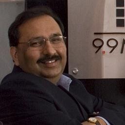
Vikas Gupta
Work:
9.9 Media - Co-founder & Director (2007)
ABP Pvt Ltd - CMO & President - Ad Sales (2006-2007)
The Coca-Cola Company - Sr. Vice President & CMO (1994-2006)
Procter & Gamble India - Marketing Manager (1988-1994)
Brooke Bond India - Product Executive (1984-1986)
ABP Pvt Ltd - CMO & President - Ad Sales (2006-2007)
The Coca-Cola Company - Sr. Vice President & CMO (1994-2006)
Procter & Gamble India - Marketing Manager (1988-1994)
Brooke Bond India - Product Executive (1984-1986)
Education:
Xavier Labour Relations Institute - Marketing & Finance, Hindu College, Univ of Delhi - Mathematics, Delhi Public School, R.K. Puram - Science

Vikas Gupta
Work:
RGPV - Lecture (14)
Education:
COP IPS Academy Indore - M. Pharm (pharmaceutics), Seth g l bihani sd college of tech edu , sriganganagar - B,pharm, Sardar children's school, jodhpur - Secondry, Central Academy, Jodhpur - Vi, National Public School, Jodhpur - Primary
About:
This is vikas gupta from jodhpur currently working as Assistant.prof. in safe institute of pharmacy, Indore
Tagline:
Jio dil se......

Vikas Gupta
Work:
MindTree - General Manager (2010)
Stealth Startup - Lead Program Manager (2009-2010)
Microsoft - Sr. Program Manager (2007-2009)
Infosys - Group Manager (2005-2007)
ISOFT - Program Manager (2003-2005)
Stealth Startup - Lead Program Manager (2009-2010)
Microsoft - Sr. Program Manager (2007-2009)
Infosys - Group Manager (2005-2007)
ISOFT - Program Manager (2003-2005)
Education:
D. Y. Patil College of Engineering, Pune - Elecrtonics
About:
A happy go lucky thinker!

Vikas Gupta
Work:
Futures First Info Services Private Limited - Forex Trader (14)
Education:
KIrori Mal College - Commerce, Budha Dal Public School - Commerce, PDS Vidya Mandir
Tagline:
ONE MoRe SoCial nEt WoRkIng SiTE :)
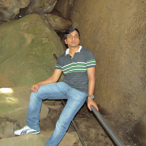
Vikas Gupta
Work:
Wipro Technologies - Senior Software Engineer (2011)
Honeywell - Senior Software Engineer (2009-2011)
Honeywell - Senior Software Engineer (2009-2011)
Education:
Ambala College of Engingeering And Appplied Research - ECE, S. D. Senior Secondary School - Non-Medical

Vikas Gupta
Work:
MoEF (NIC department) - Trainee (4)
GDG Noida
GDG Noida
Education:
SJS - All, DPS - Science (non medical)
Tagline:
A biological Living Organism

Vikas Gupta
Work:
BNP Paribas - Assistant Vice President (2005)
I-flex Solutions - Associate Consultant (2001-2005)
I-flex Solutions - Associate Consultant (2001-2005)
Education:
Indian Institute of Management Calcutta - EPGBM, National Institute of Technology Calicut - Mechanical Engineering

Vikas Gupta
Work:
ACE Teleshop - Media Coordinator (2010)
Education:
University of Delhi - Arts
About:
Graphic Designer
Classmates

Vikas Gupta
view sourceSchools:
Jodhpur University High School Jodhpur India 1997-2001

Vikas Gupta
view sourceSchools:
Jodhpur University High School Jodhpur India 1987-1991

Vikas Gupta
view sourceSchools:
Chinmaya Vidyalaya Amer. High School Cochin India 1981-1985

Vikas Gupta (Vikas)
view sourceSchools:
Anna High School Anna TX 1996-2000
Community:
Irina Nikolaevna, Brian Johnson, April Stephens, Tommy Thompson, Jeremiah Laroe, Bradley Harroff, Josh Deaton, Donald Moncier, J W, Mary Fedak

University of Waterloo - ...
view sourceGraduates:
Vikas Gupta (1986-1991),
Leslie Coo (1977-1982),
Andrea Secord (1998-2003),
Margaret Ratz (1993-1998)
Leslie Coo (1977-1982),
Andrea Secord (1998-2003),
Margaret Ratz (1993-1998)

Tri-County Regional Vocat...
view sourceGraduates:
Anna Digenni (1981-1985),
Michael Plourde (1981-1985),
Tom Powers Powers (1986-1990),
Garrett Nourse (1996-2000),
Vikas Gupta (1990-1994)
Michael Plourde (1981-1985),
Tom Powers Powers (1986-1990),
Garrett Nourse (1996-2000),
Vikas Gupta (1990-1994)
Youtube

Kumar Vikas Gupta
view source
Vikas Rattan Gupta
view source
Vikky Vikas Gupta
view source
Vikas Gupta Vicky
view source
Vikas Gupta Vikas Gupta
view source
Vikas Gupta Kumar
view source
Vikas Chandra Gupta
view source
Vikas Kumar Gupta
view sourceGet Report for Vikas B Gupta from Holly Springs, NC, age ~45


