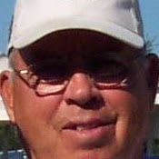
William A Harshbarger
age ~56
from Charleston, SC
- Also known as:
-
- Bill A Harshbarger
- William A Harshbar
- Wm Harshbarger
William Harshbarger Phones & Addresses
- Charleston, SC
- Napa, CA
- Saint Helena, CA
- Oakland, CA
- 15050 Al Highway 51, Opelika, AL 36804 • 3347420159
- 15084 Al Highway 51, Opelika, AL 36804 • 3347420159
- 9512 Al Highway 51, Opelika, AL 36804 • 3347420159
- Sarasota, FL
- Thonotosassa, FL
- Tampa, FL
- 15084 Al Highway 51, Opelika, AL 36804 • 3347495413
Work
-
Position:Precision Production Occupations
Education
-
Degree:Associate degree or higher
Us Patents
-
Method And Apparatus For Enhancing Chamber Cleaning
view source -
US Patent:6432255, Aug 13, 2002
-
Filed:Jan 31, 2000
-
Appl. No.:09/494581
-
Inventors:Sheng Sun - Fremont CA
Quanyuan Shang - Saratoga CA
William R. Harshbarger - San Jose CA
Robert I. Greene - Fremont CA -
Assignee:Applied Materials, Inc. - Santa Clara CA
-
International Classification:H05H 100
-
US Classification:156345, 118723 MP, 118723 MW, 118723 E
-
Abstract:A system for processing substrates within a chamber and for cleaning accumulated material from chamber components is provided. The system includes a reactive species generator adapted to generate a reactive gas species for chemically etching accumulated material from chamber components, and a processing chamber having at least one component with a mirror polished surface which is exposed to the reactive species. Preferably to have the greatest impact on chamber cleaning efficiency, the mirror polished surface is a surface of a component such as a gas distribution plate or a backing plate, and/or is a surface of a plurality of smaller components (e. g. , chamber wall liners, a gas conductance line, etc. ) so as to constitute a large percentage of the surface area exposed to the reactive species. Most preferably all bare aluminum surfaces which the reactive species contacts are mirror polished.
-
Plasma Display Panel With A Low K Dielectric Layer
view source -
US Patent:6610354, Aug 26, 2003
-
Filed:Jun 18, 2001
-
Appl. No.:09/886174
-
Inventors:Kam S. Law - Union City CA
Quanyuan Shang - Saratoga CA
Takako Takehara - Hayward CA
Taekyung Won - San Jose CA
William R. Harshbarger - San Jose CA
Dan Maydan - Los Altos Hills CA -
Assignee:Applied Materials, Inc. - Santa Clara CA
-
International Classification:C23C 1640
-
US Classification:427 68, 427579, 42725517, 42725537
-
Abstract:A plasma display panel including a low k dielectric layer. In one embodiment, the dielectric layer is comprises a fluorine-doped silicon oxide layer such as an SiOF layer. In another embodiment, the dielectric layer comprises a Black Diamondâ layer. In certain embodiments, a capping layer such as SiN or SiON is deposited over the dielectric layer.
-
Method Of Annealing Large Area Glass Substrates
view source -
US Patent:6610374, Aug 26, 2003
-
Filed:Sep 10, 2001
-
Appl. No.:09/954797
-
Inventors:Takako Takehara - Hayward CA
Regina Qiu - Cupertino CA
Yvonne LeGrice - Mountain View CA
William Reid Harshbarger - San Jose CA
Robert McCormick Robertson - Santa Clara CA -
Assignee:Applied Materials, Inc. - Santa Clara CA
-
International Classification:B05D 306
-
US Classification:427554, 427109, 427167, 42725518, 427314, 427379, 4273762
-
Abstract:A thin film layer can be formed on a glass substrate by preheating the substrate, depositing an amorphous silicon precursor layer on the substrate at a first temperature, and annealing the substrate in a thermal processing chamber at a second temperature sufficiently higher than the first temperature to substantially reduce the hydrogen concentration in the precursor layer. The preheating and annealing steps can occur in the same thermal processing chamber. Then the precursor layer is converted to a polycrystaline silicon layer by laser annealing.
-
Deposition Of Film Layers By Alternately Pulsing A Precursor And High Frequency Power In A Continuous Gas Flow
view source -
US Patent:6825134, Nov 30, 2004
-
Filed:Sep 24, 2002
-
Appl. No.:10/254627
-
Inventors:Kam S. Law - Union City CA
Quanyuan Shang - Saratoga CA
William R. Harshbarger - San Jose CA
Dan Maydan - Los Altos Hills CA
Soo Young Choi - Fremont CA
Beom Soo Park - San Jose CA
Sanjay Yadav - San Jose CA
John M. White - Hayward CA -
Assignee:Applied Materials, Inc. - Santa Clara CA
-
International Classification:H01L 21471
-
US Classification:438788, 427573, 427579
-
Abstract:A method of film layer deposition is described. A film layer is deposited using a cyclical deposition process. The cyclical deposition process consists essentially of a continuous flow of one or more process gases and the alternate pulsing of a precursor and energy to form a film on a substrate structure.
-
Method And Apparatus For Enhanced Chamber Cleaning
view source -
US Patent:6863077, Mar 8, 2005
-
Filed:Jul 15, 2002
-
Appl. No.:10/195718
-
Inventors:Sheng Sun - Fremont CA, US
Quanyuan Shang - Saratoga CA, US
William R. Harshbarger - San Jose CA, US
Robert I. Greene - Fremont CA, US -
Assignee:Applied Materials, Inc. - Santa Clara CA
-
International Classification:C25F003/00
-
US Classification:134 11, 134 2, 134 21, 134 221, 134 2211, 216 37, 216 67
-
Abstract:A system for processing substrates within a chamber and for cleaning accumulated material from chamber components is provided. The system includes a reactive species generator adapted to generate a reactive gas species for chemically etching accumulated material from chamber components, and a processing chamber having at least one component with a mirror polished surface which is exposed to the reactive species. Preferably to have the greatest impact on chamber cleaning efficiency, the mirror polished surface is a surface of a component such as a gas distribution plate or a backing plate, and/or is a surface of a plurality of smaller components (e. g. , chamber wall liners, a gas conductance line, etc. ) so as to constitute a large percentage of the surface area exposed to the reactive species. Most preferably all bare aluminum surfaces which the reactive species contacts are mirror polished.
-
Deposition Of Passivation Layers For Active Matrix Liquid Crystal Display (Amlcd) Applications
view source -
US Patent:6869838, Mar 22, 2005
-
Filed:Apr 9, 2002
-
Appl. No.:10/118864
-
Inventors:Kam Law - Union City CA, US
Quanyuan Shang - Saratoga CA, US
William Reid Harshbarger - San Jose CA, US
Dan Maydan - Los Altos Hills CA, US -
Assignee:Applied Materials, Inc. - Santa Clara CA
-
International Classification:H01L027/10
-
US Classification:438207, 438612, 438243, 438386, 257374
-
Abstract:A method of passivation layer deposition using a cyclical deposition process is described. The cyclical deposition process may comprise alternately adsorbing a silicon-containing precursor and a reactant gas on a substrate structure. Thin film transistors, such as a bottom-gate transistor or a top-gate transistor, including a silicon-containing passivation layer, may be formed using such cyclical deposition techniques.
-
Plasma Display Panel With A Low K Dielectric Layer
view source -
US Patent:7122962, Oct 17, 2006
-
Filed:Jun 11, 2003
-
Appl. No.:10/460837
-
Inventors:Kam S. Law - Union City CA, US
Quanyuan Shang - Saratoga CA, US
Takako Takehara - Hayward CA, US
Taekyung Won - San Jose CA, US
William R. Harshbarger - San Jose CA, US
Dan Maydan - Los Altos Hills CA, US -
Assignee:Applied Materials, Inc. - Santa Clara CA
-
International Classification:H01J 17/49
-
US Classification:313586, 313587
-
Abstract:A plasma display panel including a low k dielectric layer. In one embodiment, the dielectric layer is comprises a fluorine-doped silicon oxide layer such as an SiOF layer. In another embodiment, the dielectric layer comprises a Black Diamond™ layer. In certain embodiments, a capping layer such as SiN or SiON is deposited over the dielectric layer.
-
Deposition Of Silicon Layers For Active Matrix Liquid Crystal Display (Amlcd) Applications
view source -
US Patent:7439191, Oct 21, 2008
-
Filed:Apr 5, 2002
-
Appl. No.:10/117692
-
Inventors:Kam Law - Union City CA, US
Quanyuan Shang - Saratoga CA, US
William Reid Harshbarger - San Jose CA, US
Dan Maydan - Los Altos Hills CA, US -
Assignee:Applied Materials, Inc. - Santa Clara CA
-
International Classification:H01L 21/31
-
US Classification:438758, 438149, 438485, 438761, 257E21561
-
Abstract:A method of silicon layer deposition using a cyclical deposition process. The cyclical deposition process comprises alternately adsorbing a silicon-containing precursor and a reducing gas on a substrate structure. Thin film transistors, such as for example a bottom-gate transistor or a top-gate transistor, including one or more silicon layers may, be formed using such cyclical deposition techniques.
Name / Title
Company / Classification
Phones & Addresses
VALUE VIDEO INC
License Records
William R Harshbarger
License #:
3386 - Active
Category:
Emergency Medical Care
Issued Date:
Jan 3, 2013
Effective Date:
Jan 3, 2013
Expiration Date:
Dec 31, 2018
Type:
Emergency Medical Responder
Resumes

William Harshbarger
view source
William Harshbarger
view sourceLocation:
United States
Medicine Doctors

William T. Harshbarger
view sourceSpecialties:
Emergency Medicine
Work:
Aurora St Lukes Medical Center Emergency
2900 W Oklahoma Ave, Milwaukee, WI 53215
4146495550 (phone), 4146497988 (fax)
2900 W Oklahoma Ave, Milwaukee, WI 53215
4146495550 (phone), 4146497988 (fax)
Education:
Medical School
Indiana University School of Medicine
Graduated: 1998
Indiana University School of Medicine
Graduated: 1998
Languages:
English
Description:
Dr. Harshbarger graduated from the Indiana University School of Medicine in 1998. He works in Milwaukee, WI and specializes in Emergency Medicine. Dr. Harshbarger is affiliated with Aurora Sinai Medical Center and Aurora St Lukes Medical Center.
Youtube
Classmates

William Harshbarger
view sourceSchools:
Weiser High School Weiser ID 2003-2007
Community:
Donna Morgan, Shannon Dehaas
Flickr
Googleplus

William Harshbarger

William Harshbarger

William Harshbarger
Get Report for William A Harshbarger from Charleston, SC, age ~56


