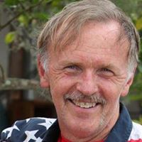
Roy M Carlson
Deceased
from Willmar, MN
Roy Carlson Phones & Addresses
- Willmar, MN
- Plymouth, MN
Medicine Doctors

Roy D. Carlson
view sourceSpecialties:
Otolaryngology, Plastic Surgery within the Head & Neck
Work:
Associates In ENT Facial Plastic SurgeryAdvanced ENT
200 Bowman Dr STE D285, Voorhees, NJ 08043
8566024000 (phone), 8569461747 (fax)
Associates In ENT Facial Plastic SurgeryAdvanced Ear Nose & Throat
239 Hurffville Crosskeys Rd STE 265, Sewell, NJ 08080
8566024000 (phone), 8566293391 (fax)
Associates In ENT Facial Plastic SurgeryAdvanced Ear Nose & Throat
204 Ark Rd STE 102, Mount Laurel, NJ 08054
8566024000 (phone), 8567784131 (fax)
Education:
Medical School
Yale University School of Medicine
Graduated: 1979
Yale University School of Medicine
Graduated: 1979
Procedures:
Allergy Testing
Hearing Evaluation
Inner Ear Tests
Sinus Surgery
Tracheostomy
Hearing Evaluation
Inner Ear Tests
Sinus Surgery
Tracheostomy
Conditions:
Acute Sinusitis
Allergic Rhinitis
Chronic Sinusitis
Deviated Nasal Septum
Hearing Loss
Allergic Rhinitis
Chronic Sinusitis
Deviated Nasal Septum
Hearing Loss
Languages:
Chinese
English
Spanish
English
Spanish
Description:
Dr. Carlson graduated from the Yale University School of Medicine in 1979. He works in Mount Laurel, NJ and 2 other locations and specializes in Otolaryngology and Plastic Surgery within the Head & Neck. Dr. Carlson is affiliated with Kennedy Health System Cherry Hill, Virtua Berlin, Virtua Marlton Hospital, Virtua Memorial Hospital and Virtua Voorhees Hospital.
Name / Title
Company / Classification
Phones & Addresses
Manager
Auto Rescue, Inc.
Auto Services. Towing - Automotive
Auto Services. Towing - Automotive
3164 Ryan Ln, Saint Paul, MN 55117
6517734025
6517734025
Operations
Budget Towing Inc of St. Paul
Budget Towing Inc
Towing - Automotive
Budget Towing Inc
Towing - Automotive
560 Randolph Ave, Saint Paul, MN 55102
6517718817, 6517713459
6517718817, 6517713459
Director
The First United Methodist Church of Hereford, Texas
Operations
Budget Towing Inc of St. Paul
Towing
Towing
560 Randolph Ave, Saint Paul, MN 55102
6517718817, 6517713459, 6122000496
6517718817, 6517713459, 6122000496
Principal
Absolute Entertainment Inc
Entertainer/Entertainment Group
Entertainer/Entertainment Group
1337 Reaney Ave, Saint Paul, MN 55106
Resumes

Roy Carlson
view sourceLocation:
United States

Roy Carlson
view sourceLocation:
United States

Engineering Manager At Broadcom
view sourcePosition:
Engineering Manager at Broadcom
Location:
Greater Minneapolis-St. Paul Area
Industry:
Semiconductors
Work:
Broadcom since Apr 2007
Engineering Manager
Engineering Manager

Roy Carlson
view sourceLocation:
United States
Work:
Science Applications International Corp. Sep 1995 - Dec 1999
Vice President
Southern Pacific Transportation Co 1990 - 1995
Vice President
Southern Pacific Transportation Jul 1962 - Jun 1990
Systems Analyst - Manager
Vice President
Southern Pacific Transportation Co 1990 - 1995
Vice President
Southern Pacific Transportation Jul 1962 - Jun 1990
Systems Analyst - Manager
Education:
Stanford University Graduate School of Business 1964 - 1966
MBA, Information Technology Purdue University 1958 - 1962
BS, Mathematics
MBA, Information Technology Purdue University 1958 - 1962
BS, Mathematics

Roy Carlson
view sourceLocation:
United States

Roy Carlson
view sourceLocation:
United States

Roy Carlson
view sourceLocation:
United States
Isbn (Books And Publications)


License Records
Roy F Carlson
License #:
122911 - Expired
Issued Date:
Jun 11, 1990
Expiration Date:
Jan 23, 1997
Type:
Salesperson
Roy E Carlson
License #:
3823 - Expired
Category:
Water Operator
Issued Date:
Oct 5, 2007
Effective Date:
Jan 9, 2012
Expiration Date:
Dec 31, 2011
Type:
Grade IV Water Operator
Us Patents
-
System Level Hardening Of Asynchronous Combinational Logic
view source -
US Patent:6791362, Sep 14, 2004
-
Filed:Dec 9, 2003
-
Appl. No.:10/731387
-
Inventors:Roy M. Carlson - Plymouth MN
David O. Erstad - Minnetonka MN -
Assignee:Honeywell International Inc. - Morristown NJ
-
International Classification:H03K 1900
-
US Classification:326 93, 326 14, 326 38
-
Abstract:A system and method for hardening an asynchronous combinational logic circuit against Single Event Upset (SEU) is presented. The asynchronous combinational logic circuit is located between two asynchronous registers. A fault detector is used to detect a fault at an output of the asynchronous combinational logic circuit caused by SEU. If the fault detector detects a fault, a first asynchronous register is prevented from clearing stored data and a second asynchronous register is prevented from loading data from the asynchronous combinational logic circuit until the fault is cleared. Further, a timer circuit is used to ensure enough time elapses to allow the asynchronous combinational logic circuit to reevaluate itself. The asynchronous combinational logic circuit reevaluates itself by first propagating a NULL wave front to clear the fault and then propagating the data stored in the first asynchronous register to its outputs.
-
Single Event Hardening Of Null Convention Logic Circuits
view source -
US Patent:6937053, Aug 30, 2005
-
Filed:Jun 17, 2003
-
Appl. No.:10/463794
-
Inventors:Roy M. Carlson - Plymouth MN, US
David O. Erstad - Minnetonka MN, US -
Assignee:Honeywell International Inc. - Morristown NJ
-
International Classification:H03K019/007
-
US Classification:326 14, 326121, 326 93
-
Abstract:A system and method for hardening a Null Convention Logic (NCL) circuit against Single Event Upset (SEU) is presented. Placing a resistive element into a feedback loop of the NCL circuit may harden the NCL circuit. A bypass element may be placed in parallel with the resistive element to increase the latching speed of the hardened NCL circuit. Additionally, replacing transistors in an input driver, the feedback loop, and an inverter with transistor stacks, which may include two or more transistors connected in series, may harden the NCL circuit. Further, two NCL gates may be cross-coupled to harden the NCL circuit.
-
Single Event Upset Hardened Circuitry Without Sensitivity To Overshoot And/Or Undershoot Conditions
view source -
US Patent:7215135, May 8, 2007
-
Filed:Dec 2, 2004
-
Appl. No.:11/002163
-
Inventors:Roy Carlson - Plymouth MN, US
-
Assignee:Honeywell International Inc. - Morristown NJ
-
International Classification:H03K 19/007
H03K 19/003 -
US Classification:326 14, 326 13, 326 23
-
Abstract:An apparatus for hardening logic circuitry against a Single-Event-Effect condition and for providing immunity to an overshoot and undershoot condition is provided. The apparatus includes undershoot-blocking and overshoot-blocking modules that are configured to be coupled to overshoot-insensitive and undershoot-insensitive nodes of the logic circuitry, respectively. The undershoot-blocking module is operable to (i) receive from a first node of the logic circuitry a first signal event having a undershoot condition impressed thereon, and (ii) block it from passing to the overshoot-insensitive node. The overshoot-blocking module is operable to (i) receive from the first node a second signal event having an overshoot condition impressed thereon, and (ii) block it from passing to the undershoot-insensitive node. As such, further propagation of the overshoot and undershoot conditions are prevented.
-
Error Recovery In Asynchronous Combinational Logic Circuits
view source -
US Patent:7451384, Nov 11, 2008
-
Filed:Jul 15, 2004
-
Appl. No.:10/891654
-
Inventors:David O. Erstad - Minnetonka MN, US
Roy M. Carlson - Plymouth MN, US -
Assignee:Honeywell International Inc. - Morristown NJ
-
International Classification:G06F 11/08
-
US Classification:714797, 714789, 365181, 326 35
-
Abstract:A system and method for providing error recovery to an asynchronous logic circuit is presented. The asynchronous logic circuit with error recovery may use temporal redundancy to compare the results of an asynchronous computation and initiate error recovery if necessary. Outputs of the asynchronous logic circuit are compared using a plurality of asynchronous register voters. If an asynchronous register voter detects an inconsistent result, the asynchronous register voter clears itself. A majority of common data outputs from the plurality of asynchronous register voters is provided as an output that is representative of the output of the asynchronous logic circuit.
-
Digital Single Event Transient Hardened Register Using Adaptive Hold
view source -
US Patent:7619455, Nov 17, 2009
-
Filed:Apr 19, 2007
-
Appl. No.:11/737225
-
Inventors:Roy M. Carlson - Plymouth MN, US
David O. Erstad - Minnetonka MN, US -
Assignee:Honeywell International Inc. - Morristown NJ
-
International Classification:H03K 3/356
-
US Classification:327212, 327199, 327201
-
Abstract:By adjusting a register's capturing clock edge timing so that the register captures data when the data returns to a correct state, the register may be protected against DSET upsets. If a data glitch occurs near the clock edge, the valid time at the register output is increased (CLK to Q). This valid time increase occurs when the presence of a DSET transient is detected near the clock edge.
-
One-Time Programmable Memory Cell
view source -
US Patent:8031506, Oct 4, 2011
-
Filed:Mar 21, 2008
-
Appl. No.:12/077888
-
Inventors:Jonathan Schmitt - Eden Prairie MN, US
Roy Carlson - Plymouth MN, US -
Assignee:Broadcom Corporation - Irvine CA
-
International Classification:G11C 17/16
-
US Classification:365 96, 257530, 257209
-
Abstract:A disclosed embodiment is a programmable memory cell having improved IV characteristics comprising a thick oxide spacer transistor interposed between a programmable thin oxide antifuse and a thick oxide access transistor. The spacer transistor separates a rupture site formed during programming the programmable antifuse from the access transistor, so as to result in the improved IV characteristics. The programmable antifuse is proximate to one side of the spacer transistor, while the access transistor is proximate to an opposite side of the spacer transistor. The source region of the access transistor is coupled to ground, and the drain region of the access transistor also serves as the source region of the spacer transistor. The access transistor is coupled to a row line, while the spacer transistor and the programmable antifuse are coupled to a column line. The rupture site is formed during programming by applying a programming voltage to the programmable antifuse.
-
Radiation Hardening Of Logic Circuitry Using A Cross Enabled, Interlocked Logic System And Method
view source -
US Patent:20050156620, Jul 21, 2005
-
Filed:Jan 15, 2004
-
Appl. No.:10/759913
-
Inventors:Roy Carlson - Plymouth MN, US
-
Assignee:Honeywell International Inc. - Morristown NJ
-
International Classification:H03K019/003
-
US Classification:326010000
-
Abstract:A system and method for hardening a logic circuit against radiation-event effects is provided. The system may include a logic circuit, first and second feed-forward devices, and first and second feedback devices. The logic circuit may be operable to output independently-obtained first and second redundant signals responsive to a desired input signal. Each of the first and second feed-forward devices may receive both of the first and second redundant signals. When the first and second redundant signals are in expected states, then the first and second feed-forward devices may responsively provide respective first and second feed-forward signals. Each of the first and second feedback devices may receive both of the first and second feed-forward signals. When the first and second feed-forward signals are in expected states, then the first and second feedback devices responsively feed respective first and second feedback signals back to the respective first and second redundant signals.
-
Pulse-Rejecting Circuit For Suppressing Single-Event Transients
view source -
US Patent:20060119410, Jun 8, 2006
-
Filed:Dec 6, 2004
-
Appl. No.:11/005265
-
Inventors:Roy Carlson - Plymouth MN, US
-
Assignee:Honeywell International Inc. - Morristown NJ
-
International Classification:H03K 5/08
-
US Classification:327310000
-
Abstract:A circuit for rejecting single-event transients (SETs) from logic signals is provided. The circuit includes a delay circuit, an inverter circuit, and an output-holding circuit. The delay circuit receives an input signal and delays the input signal to produce a time-delayed version of the input signal. The input signal and the time-delayed version of the input signal are fed into the inverter circuit that propagates a corresponding output signal only when the input signal and the time-delayed version of the input signal have the same logic level. If the input signal or the time-delayed version of the input signal transitions such that both input signals presented to the inverter circuit have opposite logic levels, the output-holding circuit maintains the output signal in its previous state.
Lawyers & Attorneys

Roy L. Carlson, Jr. - Lawyer
view sourceOffice:
Milberg & DePhillips Professional Corporation
Phone:
7609437103 (Phone)
Specialties:
Bankruptcy
Corporate Reorganization
Creditors Rights
Business Litigation
Trademark Registration
Business Transactions
Business Start-Ups
Appellate Practice
Real Estate
Corporate Reorganization
Creditors Rights
Business Litigation
Trademark Registration
Business Transactions
Business Start-Ups
Appellate Practice
Real Estate
Memberships:
San Diego County (Chair, Local Bankruptcy Rules Revision Committee, 1994-1996
Member, Bankruptcy Section
Mentor, Mentoring Program) and American (Member: Lawyers Conference Committee of Judicial Performance and Conduct Committee, 1996-1998) Bar Associations
State Bar of California
U.S. Bankruptcy Court for the Southern District of California (Member, Electronic Filing Committee
Co-Chair, CM/ECF Main User Group
Chair, CM/ECF Local Rules Revision Committee).
ISLN:
908535260
Admitted:
1986, California and U.S. District Court, Southern District of California
1992, U.S. District Court, Central District of California
1995, U.S. District Court, District of Arizona, U.S. Court of Appeals, Ninth Circuit and U.S. Supreme Court
2001, U.S. District Court, Northern District of California
2004, U.S. District Court, District of Colorado, U.S. Court of Appeals, Tenth Circuit
2009, U.S. District Court, Eastern District of California
University:
University of California at San Diego, B.A., with honors, 1980
Law School:
Thomas Jefferson School of Law, J.D., with scholastic merit, 1985
Reported:
In re Consolidated Pioneer Mortgage, 178 B.R. 222 (9th Cir. BAP 1995); In re Casey, 193 B.R. 942 (Bkrptcy. S.D., Cal. 1996); In re Casey, 198 B.R. 918 (Bkrptcy., S.D., Cal., 1996); Coscia v. McKenna & Cuneo (2000) 80 Cal. App. 4th 617; Coscia v. McKenna & Cuneo (2001) 25 Cal. 4th 1194.
Biography:
Recipient, American Jurisprudence Award in Criminal Law. Member, Criminal Justice Journal, 1985. Law Clerk, Hon. John J. Hargrove, Judge, U.S. Bankruptcy Court, Southern District of California, 1988-1...
News

Ice Age Death Rituals Revealed at Infant Burial Site
view source- "They were treating the human remains with respect, and that's really what you need to do," said Roy Carlson, professor emeritus of archaeology at Simon Fraser University in British Columbia, Canada, who was not involved in the study.
- Date: Nov 10, 2014
- Category: Sci/Tech
- Source: Google

Roy Carlson
view source
Roy Carlson
view source
Roy Carlson
view source
Roy Carlson
view source
Roy Carlson
view source
Roy Peter Carlson
view source
Roy Carlson
view source
Roy L Carlson
view sourceClassmates

Roy Carlson
view sourceSchools:
Mills Elementary School Crawfordsville IN 1946-1948, Saint Thomas Aquinas School Indianapolis IN 1948-1950, James W. Riley School 43 Indianapolis IN 1951-1954
Community:
Ted Levee, Mark Leavell, Darlene Barnett

Roy Carlson
view sourceSchools:
Mount Oliver School Pittsburgh PA 1953-1962
Community:
Theresa Bogaski, Donna Reich

Roy Carlson (Roy)
view sourceSchools:
Northeast High School San Antonio TX 2003-2007
Community:
Norma Williamson, Judith Irick, Turner Reid

Roy Chip Carlson
view sourceSchools:
Grover Cleveland High School Caldwell NJ 1951-1955
Community:
Laura Moor, H Wagner, Gary Kelly, Diane Bothem, Cyril Levine, Donna Kelly

Roy Carlson
view sourceSchools:
Waukesha High School (thru 1974) Waukesha WI 1952-1956
Community:
Denise Davis, Karen Toycen, Michael Hagen

Roy Carlson
view sourceSchools:
Greer High School Hoopeston IL 1942-1946
Community:
Michael Curry, Linda Santillana, Mike Brewster

Roy Carlson
view sourceSchools:
St. Philomena School East Cleveland OH 1946-1954
Community:
Yasmeen Thomas, Jeanne Guthrie, Janet Graves, Jim Forristal
Myspace
Youtube
Googleplus

Roy Carlson
Work:
Cell-Express - Sales
Tagline:
Ya Tu Saves

Roy Carlson
Education:
TAW matric hr sec school

Roy Carlson

Roy Carlson

Roy Carlson

Roy Carlson

Roy Carlson

Roy Carlson
Get Report for Roy M Carlson from Willmar, MNDeceased


