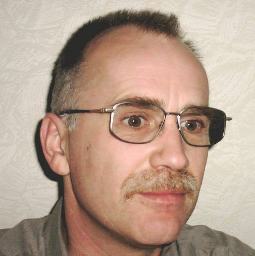
Peter J Gruber
age ~76
from Sea Cliff, NY
- Also known as:
-
- Peter Dr Gruber
- Peter G Gruber
- Gail Marie Gruber
- Peter J Grube
- Phone and address:
-
52 Prospect Ave, Sea Cliff, NY 11542
5167597721
Peter Gruber Phones & Addresses
- 52 Prospect Ave, Sea Cliff, NY 11542 • 5167597721
- 17 Tanglewood Ln, Sea Cliff, NY 11579
- Holbrook, NY
- 40 Wooleys Ln, Great Neck, NY 11023 • 5164822183
- Nassau, NY
- Floral Park, NY
Work
-
Company:WEILER DIVISION-MONTEFIORE HOSPITAL
-
Address:1825 Eastchester Rd, Bronx, NY 10461
-
Phones:7189206626 7189042517
Education
-
School / High School:New York Medical College1988
Languages
English
Awards
Healthgrades Honor Roll
Ranks
-
Certificate:Emergency Medicine, 2004
Specialities
Emergency Medicine
Lawyers & Attorneys

Peter Gruber - Lawyer
view sourceOffice:
Slingerland & Clark, P.C.
Specialties:
Criminal Defense
Criminal Defense
Criminal Defense
ISLN:
917231757
Admitted:
1991
Law School:
Loyola University, J.D.
Us Patents
-
Common Ball-Limiting Metallurgy For I/O Sites
view source -
US Patent:6534863, Mar 18, 2003
-
Filed:Feb 9, 2001
-
Appl. No.:09/781121
-
Inventors:George F. Walker - New York NY
Ronald D. Goldblatt - Yorktown Heights NY
Peter A. Gruber - Mohegan Lake NY
Raymond R. Horton - Dover Plains NY
Kevin S. Petrarca - Newburgh NY
Richard P. Volant - New Fairfield CT
Tien-Jen Cheng - Bedford NY -
Assignee:International Business Machines Corporation - Armonk NY
-
International Classification:H01L 2348
-
US Classification:257737, 257751, 257761, 257762, 257766, 257769, 257781, 257784
-
Abstract:A process is described for forming a common input-output (I/O) site that is suitable for both wire-bond and solder bump flip chip connections, such as controlled-collapse chip connections (C4). The present invention is particularly suited to semiconductor chips that use copper as the interconnection material, in which the soft dielectrics used in manufacturing such chips are susceptible to damage due to bonding forces. The present invention reduces the risk of damage by providing site having a noble metal on the top surface of the pad, while providing a diffusion barrier to maintain the high conductivity of the metal interconnects. Process steps for forming an I/O site within a substrate are reduced by providing a method for selectively depositing metal layers in a feature formed in the substrate. Since the I/O sites of the present invention may be used for either wire-bond or solder bump connections, this provides increased flexibility for chip interconnection options, while also reducing process costs.
-
Global Vacuum Injection Molded Solder System And Method
view source -
US Patent:7497366, Mar 3, 2009
-
Filed:Jun 6, 2007
-
Appl. No.:11/758752
-
Inventors:S. Jay Chey - Ossining NY, US
Steven A. Cordes - Yorktown Heights NY, US
Peter A. Gruber - Mohegan Lake NY, US
John U. Knickerbocker - Monroe NY, US
James L. Speidell - Poughquag NY, US -
Assignee:International Business Machines Corporation - Armonk NY
-
International Classification:B23K 31/02
-
US Classification:228256, 228200
-
Abstract:A system and method are provided for injection molding conductive bonding material into a plurality of cavities in a mold within a vacuum chamber. A mold and a fill head are located within a vacuum chamber, wherein the mold includes a plurality of cavities. A vacuum is created within the vacuum chamber, thereby removing air from the chamber and from the cavities. Optionally, rotational motion is provided to at least one of the mold and the fill head while the fill head is in substantial contact with the mold. Conductive bonding material is forced out of the fill head toward the mold, and into at least one of the cavities, while a vacuum is maintained in the vacuum chamber.
-
Techniques For Forming Solder Bump Interconnects
view source -
US Patent:8148255, Apr 3, 2012
-
Filed:Sep 18, 2007
-
Appl. No.:11/856831
-
Inventors:Bing Dang - Chappaqua NY, US
Peter A. Gruber - Mohegan Lake NY, US
Luc Guerin - Quebec, CA
Chirag S. Patel - Peerkskill NY, US -
Assignee:International Business Machines Corporation - Armonk NY
-
International Classification:H01L 21/44
-
US Classification:438613, 438106, 438615, 438616, 257E21575, 257E2301
-
Abstract:Interconnects are formed on attachment points of a wafer by performing several steps. A plurality of cavities having a predetermined shape is formed in a semiconductor substrate. These cavities are then filled with an interconnect material to form the interconnects. The interconnects are subsequently attached to the attachment points of the wafer.
-
Sprocket Opening Alignment Process And Apparatus For Multilayer Solder Decal
view source -
US Patent:8268719, Sep 18, 2012
-
Filed:Jan 1, 2011
-
Appl. No.:12/983292
-
Inventors:Stephen L. Buchwalter - Armonk NY, US
Peter A. Gruber - Armonk NY, US
Jae-Woong Nah - Armonk NY, US
Da-Yuan Shih - Poughkeepsie NY, US -
Assignee:International Business Machines Corporation - Armonk NY
-
International Classification:H01L 21/44
-
US Classification:438616, 257E21506, 29843, 22818022
-
Abstract:A process for aligning at least two layers in an abutting relationship with each other comprises forming a plurality of sprocket openings in each of the layers for receiving a sprocket of diminishing diameters as the sprocket extends outwardly from a base, with the center axes of the sprocket openings in each layer being substantially alignable with one another, the diameter of the sprocket openings in an abutting layer for first receiving the sprocket being greater than the diameter of the sprocket openings in an abutted layer. This is followed by forming a plurality of reservoir openings in each of at least two of the layers and positioning the sprocket openings in the layers to correspond with one another and the reservoir openings in the layers to correspond with one another so that substantial alignment of the center axes of the corresponding sprocket openings in the layers effects substantial alignment of the center axes of the corresponding reservoir openings in the layers. Engaging the sprocket openings with the sprocket by inserting the end of the sprocket having the smallest diameter into the sprocket openings having the largest diameter in the layers and continuing through to the sprocket opening having the smallest diameter in the layers effects substantial alignment of the center axes of the corresponding sprocket openings and substantial alignment of the center axes of the corresponding reservoir openings in the layers. The invention also comprises apparatus for performing this process.
-
Techniques For Forming Solder Bump Interconnects
view source -
US Patent:8328156, Dec 11, 2012
-
Filed:Feb 13, 2012
-
Appl. No.:13/371840
-
Inventors:Bing Dang - Chappaqua NY, US
Peter A. Gruber - Mohegan Lake NY, US
Luc Guerin - Quebec, CA
Chirag S. Patel - Peekskill NY, US -
Assignee:International Business Machines Corporation - Armonk NY
-
International Classification:B28B 7/22
E04G 11/50 -
US Classification:249 60, 249117, 257E21586
-
Abstract:Interconnects are formed on attachment points of a wafer by performing several steps. A plurality of cavities having a predetermined shape is formed in a semiconductor substrate. These cavities are then filled with an interconnect material to form the interconnects. The interconnects are subsequently attached to the attachment points of the wafer.
-
Common Ball-Limiting Metallurgy For I/O Sites
view source -
US Patent:20030092254, May 15, 2003
-
Filed:Dec 18, 2002
-
Appl. No.:10/322831
-
Inventors:George Walker - New York NY, US
Ronald Goldblatt - Yorktown Heights NY, US
Peter Gruber - Mohegan Lake NY, US
Raymond Horton - Dover Plains NY, US
Kevin Petrarca - Newburgh NY, US
Richard Volant - New Fairfield CT, US
Tien-Jen Cheng - Bedford NY, US -
International Classification:H01L021/44
-
US Classification:438/613000
-
Abstract:A process is described for forming a common input-output (I/O) site that is suitable for both wire-bond and solder bump flip chip connections, such as controlled-collapse chip connections (C4). The present invention is particularly suited to semiconductor chips that use copper as the interconnection material, in which the soft dielectrics used in manufacturing such chips are susceptible to damage due to bonding forces. The present invention reduces the risk of damage by providing site having a noble metal on the top surface of the pad, while providing a diffusion barrier to maintain the high conductivity of the metal interconnects. Process steps for forming an I/O site within a substrate are reduced by providing a method for selectively depositing metal layers in a feature formed in the substrate. Since the I/O sites of the present invention may be used for either wire-bond or solder bump connections, this provides increased flexibility for chip interconnection options, while also reducing process costs.
-
Injection Molded Soldering Head For High Temperature Application And Method Of Making Same
view source -
US Patent:20080014406, Jan 17, 2008
-
Filed:Jul 11, 2006
-
Appl. No.:11/484124
-
Inventors:S. Jay Chey - Ossining NY, US
Peter A. Gruber - Mohegan Lake NY, US -
International Classification:C23C 16/00
B32B 3/10 -
US Classification:428131, 4272497
-
Abstract:An injection molded soldering head includes a substrate that is flexible (compliant) and stable at high temperature. The substrate includes an aperture therethrough for holding and dispensing solder onto a mold and a low friction coating on the bottom side of the substrate to provide a lower friction surface for the head.
-
Methods Of Creating Molds Of Variable Solder Volumes For Flip Attach
view source -
US Patent:20090001248, Jan 1, 2009
-
Filed:Aug 23, 2007
-
Appl. No.:11/844070
-
Inventors:Matthew J. Farinelli - Bronx NY, US
Steven Cordes - Yorktown Heights NY, US
Donna S. Nielsen - Yorktown Heights NY, US
Samuel Roy McKnight - New Paltz NY, US
Jay S. Chey - Ossining NY, US
Peter A. Gruber - Mohegan Lake NY, US
Joanna Rosner - Cortland Manor NY, US -
International Classification:B22C 9/00
-
US Classification:249119
-
Abstract:A solder mold includes a substrate and a plurality of cavities for holding solder to be transferred to an integrated circuit. The plurality of cavities comprises cavities of at least two different volumes.
Isbn (Books And Publications)


Von Dobler Bis DV-CAM: Ergonomics Fur Amateurfilm Zur Geschichte Der Kinematographie
view sourceAuthor
Peter Gruber
ISBN #
3631340230
Name / Title
Company / Classification
Phones & Addresses
Director
Glen Rose Lions Club
Civic/Social Association
Civic/Social Association
Peter Gruber MD
Emergency Medicine
Emergency Medicine
305 E 161 St, Bronx, NY 10451
7185792500
7185792500
Chairman, Principal
Gruber Foundation
Civic/Social Association
Civic/Social Association
140 W 57 St, New York, NY 10019
PO Box 208958, New Haven, CT 06520
2122478484
PO Box 208958, New Haven, CT 06520
2122478484
Wikipedia References

Peter Gruber (Footballer)
License Records
Peter Gruber
License #:
E011934 - Expired
Category:
Emergency medical services
Issued Date:
Oct 16, 2009
Expiration Date:
Oct 31, 2011
Type:
Sierra-Sacramento Valley EMS Agency
Resumes

Advisory Engineer At Ibm Research - Retired
view sourceLocation:
Greater New York City Area
Industry:
Electrical/Electronic Manufacturing
Work:
IBM Research Feb 1978 - Jul 2011
Advisory Engineer
Advisory Engineer
Education:
Heald College 1976 - 1977
Associate, Applied Science; Electronic Engineering Technology
Associate, Applied Science; Electronic Engineering Technology
Interests:
Astronomy, Biomimetics
Languages:
German

Fo At Globaljet
view sourcePosition:
fo at globaljet
Location:
United States
Industry:
Building Materials
Work:
globaljet
fo
fo
Medicine Doctors

Dr. Peter J Gruber, Bronx NY - MD (Doctor of Medicine)
view sourceSpecialties:
Emergency Medicine
Address:
111 E 210Th St, Bronx, NY 10467
7189202323 (Phone)
WEILER DIVISION-MONTEFIORE HOSPITAL
1825 Eastchester Rd, Bronx, NY 10461
7189206626 (Phone), 7189042517 (Fax)
MONTEFIORE MEDICAL CENTER
1825 Eastchester Rd, Bronx, NY 10461
7189042500 (Phone), 7189042827 (Fax)
7189202323 (Phone)
WEILER DIVISION-MONTEFIORE HOSPITAL
1825 Eastchester Rd, Bronx, NY 10461
7189206626 (Phone), 7189042517 (Fax)
MONTEFIORE MEDICAL CENTER
1825 Eastchester Rd, Bronx, NY 10461
7189042500 (Phone), 7189042827 (Fax)
Certifications:
Emergency Medicine, 2004
Awards:
Healthgrades Honor Roll
Languages:
English
Hospitals:
111 E 210Th St, Bronx, NY 10467
WEILER DIVISION-MONTEFIORE HOSPITAL
1825 Eastchester Rd, Bronx, NY 10461
MONTEFIORE MEDICAL CENTER
1825 Eastchester Rd, Bronx, NY 10461
Jacobi Medical Center
1400 Pelham Parkway South, Bronx, NY 10461
WEILER DIVISION-MONTEFIORE HOSPITAL
1825 Eastchester Rd, Bronx, NY 10461
MONTEFIORE MEDICAL CENTER
1825 Eastchester Rd, Bronx, NY 10461
Jacobi Medical Center
1400 Pelham Parkway South, Bronx, NY 10461
Education:
Medical School
New York Medical College
Graduated: 1988
Medical School
Long Island Jewish Med Center
Graduated: 1988
New York Medical College
Graduated: 1988
Medical School
Long Island Jewish Med Center
Graduated: 1988

Peter J. Gruber
view sourceSpecialties:
Congenital Cardiac Surgery (Thoracic Surgery), Transplant Surgery
Work:
University Of Iowa Cardiac & Thoracic Surgery
200 Hawkins Dr STE SE500GH, Iowa City, IA 52242
3193563440 (phone), 3193563891 (fax)
200 Hawkins Dr STE SE500GH, Iowa City, IA 52242
3193563440 (phone), 3193563891 (fax)
Education:
Medical School
University of Pennsylvania School of Medicine
Graduated: 1992
University of Pennsylvania School of Medicine
Graduated: 1992
Languages:
English
Description:
Dr. Gruber graduated from the University of Pennsylvania School of Medicine in 1992. He works in Iowa City, IA and specializes in Congenital Cardiac Surgery (Thoracic Surgery) and Transplant Surgery. Dr. Gruber is affiliated with University Of Iowa Hospitals & Clinics.

Peter J Gruber, Bronx NY
view sourceSpecialties:
Emergency Medicine
Work:
Montefiore Medical Center
111 E 210Th St, Bronx, NY 10467
MMG-Comprehensive Family Care Center CFCC
305 E 161St St, Bronx, NY 10451
Montefiore Medical Center
600 E 233Rd St, Bronx, NY 10466
111 E 210Th St, Bronx, NY 10467
MMG-Comprehensive Family Care Center CFCC
305 E 161St St, Bronx, NY 10451
Montefiore Medical Center
600 E 233Rd St, Bronx, NY 10466
Education:
New York Medical College (1988)

Peter J Gruber, Bronx NY
view sourceSpecialties:
Emergency Medicine Physician
Address:
111 E 210Th St, Bronx, NY 10467
Board certifications:
American Board of Emergency Medicine Certification in Emergency Medicine
Plaxo

Peter Gruber
view sourceInfineon Technologies Past: Siemens AG
Googleplus

Peter Gruber
Work:
Zep Solar - Senior Product Development Engineer

Peter Gruber

Peter Gruber

Peter Gruber

Peter Gruber

Peter Gruber

Peter Gruber

Peter Gruber
Flickr

Peter Gruber
view source
Peter Gruber
view source
Peter Gruber
view source
Peter Gruber
view source
Gruber Peter
view source
Hans Peter Gruber
view source
Peter Gruber
view source
Peter Gruber
view sourceClassmates

Peter Gruber
view sourceSchools:
Middlesex High School Middlesex VA 1981-1985
Community:
Charles Cooke

Peter Gruber | Piedmont B...
view source
Peter Gruber | Foothill M...
view source
Addison Trail High School...
view sourceGraduates:
Annamarie Mancini (1987-1991),
Kristina Kolioulis (2000-2004),
Pete Gruber (1972-1976),
Robert Szuflita (1988-1992)
Kristina Kolioulis (2000-2004),
Pete Gruber (1972-1976),
Robert Szuflita (1988-1992)

Foothill Middle College, ...
view sourceGraduates:
Peter Gruber (1995-1999),
Seth Anison (2005-2009),
Gail Kirk (1992-1996),
Jerry Gaylor (1961-1972),
Evelyn Perez (2005-2009)
Seth Anison (2005-2009),
Gail Kirk (1992-1996),
Jerry Gaylor (1961-1972),
Evelyn Perez (2005-2009)
Youtube
Get Report for Peter J Gruber from Sea Cliff, NY, age ~76


