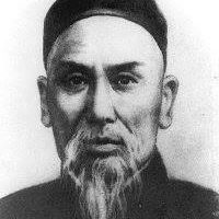
Yang Lu
age ~43
from San Francisco, CA
- Also known as:
-
- Yan G Lu
- Lu Yang
- Yang Lv
- Phone and address:
- 646 Lakeview Ave, San Francisco, CA 94112
Yang Lu Phones & Addresses
- 646 Lakeview Ave, San Francisco, CA 94112
- 770 Joost Ave, San Francisco, CA 94127
- Fremont, CA
- San Jose, CA
- Pacifica, CA
- Oakland, CA
Lawyers & Attorneys
Wikipedia

Yang Luch'an
view sourceYang Lu-ch'an or Yang Luchan, simplified Chinese: ; traditional Chinese: ; pinyin: Yng Lchn; also known as Yang Fu-k'ui (simplified Chinese: ...
Name / Title
Company / Classification
Phones & Addresses
Co-founder
Sunfire Enterprises, LLC - OutstandingPet
Sunfire Enterprises. LLC
Pet Training. Pet Supplies & Foods - Retail
Sunfire Enterprises. LLC
Pet Training. Pet Supplies & Foods - Retail
2155 Stonington Ave., Suite 108, Hoffman Estates, IL 60169
8669338429
8669338429
GOLDEN DYNASTY CHINESE RESTAURANT INC
CHINA KING OF COLUMBUS LLC
GOLDEN DYNASTY BUFFET INC
ECO-GP LTD
Resumes

Yang Lu San Francisco, CA
view sourceWork:
Deloitte Beijing Branch
Jul 2013 to Sep 2013
Intern AVIS
Jul 2012 to Jun 2013
Driver Ocean View Park and Recreation Center
May 2010 to Aug 2011
Member of soccer Team SFVITA
San Francisco, CA
Jan 2010 to Mar 2010
Volunteer City College of San Francisco
Aug 2003 to May 2006
Student Worker City College of San Francisco
San Francisco, CA
Aug 2003 to Dec 2005
Office & Administrative Support Yu Lai High School
Jan 1998 to May 2002
Member of Basketball Team
Education:
San Francisco State University
Jan 2006 to Jul 2012
Business Administration San Francisco City College
Mar 2003 to Dec 2005
Jan 2006 to Jul 2012
Business Administration San Francisco City College
Mar 2003 to Dec 2005
Medicine Doctors

Yang Sieng Lu
view sourceSpecialties:
Internal Medicine
Hematology
Hematology
Education:
Case Western Reserve University(1969)
Us Patents
-
Methods And Apparatus For Ldmos Transistors
view source -
US Patent:7868378, Jan 11, 2011
-
Filed:Jul 17, 2006
-
Appl. No.:11/488378
-
Inventors:Marco A. Zuniga - Fremont CA, US
Budong You - Fremont CA, US
Yang Lu - Fremont CA, US -
Assignee:Volterra Semiconductor Corporation - Fremont CA
-
International Classification:H01L 29/66
H01L 21/02
H01L 21/84
H01L 21/8238 -
US Classification:257328, 257492, 257493, 257339, 257557, 257611, 257E29187, 257E29261, 257E21373, 257E21452, 438163, 438204, 438236, 438327, 438335
-
Abstract:An LDMOS transistor includes a gate including a conductive material over an insulator material, a source including a first impurity region and a second impurity region, a third impurity region, and a drain including a fourth impurity region and a fifth impurity region. The first impurity region is of a first type, and the second impurity region is of an opposite second type. The third impurity region extends from the source region under the gate and is of the first type. The fourth impurity region is of the second type, the fifth impurity region is of the second type, and the fourth impurity region impinges the third impurity region.
-
Methods And Apparatus For Ldmos Transistors
view source -
US Patent:8431450, Apr 30, 2013
-
Filed:Jan 10, 2011
-
Appl. No.:12/987905
-
Inventors:Marco A. Zuniga - Fremont CA, US
Budong You - Fremont CA, US
Yang Lu - Fremont CA, US -
Assignee:Volterra Semiconductor Corporation - Fremont CA
-
International Classification:H01L 29/66
H01L 21/02
H01L 21/84
H01L 21/8238 -
US Classification:438163, 257328, 257333, 257493, 257557, 257611, 257E29187, 257E29261, 257E21373, 257E21452, 438204, 438236, 438316, 438325, 438327, 438335
-
Abstract:An LDMOS transistor includes a gate including a conductive material over an insulator material, a source including a first impurity region and a second impurity region, a third impurity region, and a drain including a fourth impurity region and a fifth impurity region. The first impurity region is of a first type, and the second impurity region is of an opposite second type. The third impurity region extends from the source region under the gate and is of the first type. The fourth impurity region is of the second type, the fifth impurity region is of the second type, and the fourth impurity region impinges the third impurity region.
-
Vertical Gate Ldmos Device
view source -
US Patent:8647950, Feb 11, 2014
-
Filed:Aug 10, 2012
-
Appl. No.:13/572428
-
Inventors:Marco A. Zuniga - Palo Alto CA, US
Yang Lu - Fremont CA, US
Badredin Fatemizadeh - Sunnyvale CA, US
Jayasimha Prasad - San Jose CA, US
Amit Paul - Sunnyvale CA, US
Jun Ruan - Santa Clara CA, US -
Assignee:Volterra Semiconductor Corporation - Fremont CA
-
International Classification:H01L 21/336
-
US Classification:438270, 438286, 438589, 257E21621
-
Abstract:A method of fabricating a vertical gate region in LDMOS transistor includes depositing a first masking layer on an n-well region implanted on a substrate, patterning the first masking layer to define an area, depositing a second masking layer over the area, etching through the second masking layer in a first portion of the area to expose the n-well region, and etching the exposed n-well region to form a first trench. The first trench, extending from a surface of the n-well region to a first depth, is filled with an oxide. The second masking layer is etched through in a second portion of the area to expose the n-well region. A second trench is formed in the n-well, the second trench extending from the surface to a second depth, less than the first depth. An asymmetric vertical gate is formed by filling the second trench with a conductive material.
-
Programmable Priority For Concurrent Multi-Threaded Processors
view source -
US Patent:20070094664, Apr 26, 2007
-
Filed:Oct 21, 2005
-
Appl. No.:11/256631
-
Inventors:Kimming So - Palo Alto CA, US
Baobinh Truong - San Jose CA, US
Yang Lu - Palo Alto CA, US
Hon-Chong Ho - Fremont CA, US
Li-Hung Chang - Santa Clara CA, US
Chia-Cheng Choung - Fremont CA, US
Jason Leonard - San Jose CA, US -
International Classification:G06F 9/46
-
US Classification:718103000
-
Abstract:A first thread processor of a multi-thread processor system is operable to execute a first process, and a second thread processor of the multi-thread processor system is operable to execute a second process. A control register is operable to store priority information that is individually associated with at least one of the first thread processor and the second thread processor. The priority information identifies a prioritization of the first thread processor and/or a restriction on the second thread processor in a use of a shared hardware resource during execution of at least one of the first process and the second process.
-
Power Transistor With Protected Channel
view source -
US Patent:20090224333, Sep 10, 2009
-
Filed:Jan 14, 2009
-
Appl. No.:12/353866
-
Inventors:Yang Lu - Fremont CA, US
Budong You - Fremont CA, US
Marco A. Zuniga - Palo Alto CA, US
Hamza Yilmaz - Saratoga CA, US -
International Classification:H01L 27/105
H01L 21/265
H01L 29/78 -
US Classification:257392, 438514, 257E29255, 257E27081, 257E21334, 257368
-
Abstract:A transistor includes a substrate, a well formed in the substrate, a drain including a first impurity region implanted in the well, a source including a second impurity region implanted in the well and spaced apart from the first impurity region, a channel for current flow from the drain to the source, and a gate to control a depletion region between the source and the drain The channel has an intrinsic breakdown voltage, and the well, drain and source are configured to provide an extrinsic breakdown voltage lower than the intrinsic breakdown voltage and such that breakdown occurs in a breakdown region in the well located outside the channel and adjacent the drain or the source.
-
Vertical Gate Ldmos Device
view source -
US Patent:20130105887, May 2, 2013
-
Filed:Aug 10, 2012
-
Appl. No.:13/572015
-
Inventors:Marco A. Zuniga - Palo Alto CA, US
Yang Lu - Fremont CA, US
Badredin Fatemizadeh - Sunnyvale CA, US
Jayasimha Prasad - San Jose CA, US
Amit Paul - Sunnyvale CA, US
Jun Ruan - Santa Clara CA, US -
Assignee:Volterra Semiconductor Corporation - Fremont CA
-
International Classification:H01L 29/78
H01L 29/66 -
US Classification:257330, 438270
-
Abstract:Described here are transistors and fabrication methods thereof. In one implementation, a transistor includes an n-well region implanted into a surface of a substrate, and a trench in the n-well region. The trench extends from the surface to a first depth. The trench includes a gate of conductive material in the trench, and dielectric material filling a volume of the trench not filled by the conductive material. The transistor also includes a p-type material in a first region extending from a second depth to a third depth, the second depth and the third depth being greater than the first depth. The transistor further includes a source region and a drain region.
-
Transistor With Buried P+ And Source Contact
view source -
US Patent:20130105888, May 2, 2013
-
Filed:Aug 10, 2012
-
Appl. No.:13/572110
-
Inventors:Marco A. Zuniga - Palo Alto CA, US
Yang Lu - Fremont CA, US
Badredin Fatemizadeh - Sunnyvale CA, US
Jayasimha Prasad - San Jose CA, US
Amit Paul - Sunnyvale CA, US
Jun Ruan - Santa Clara CA, US -
Assignee:Volterra Semiconductor Corporation - Fremont CA
-
International Classification:H01L 29/78
-
US Classification:257330, 257335
-
Abstract:The present application features a transistor that includes an n-well region implanted into a surface of a substrate, a gate region, and a source region, and a drain region. The source region is on a first side of the gate region and includes a p-body region in the n-well region. An n+ region and a p+ region are implanted in the p-body region such that the p+ region is below the n+ region. The drain region is on a second side of the gate region and includes an n+ region.
-
Vertical Gate Ldmos Device
view source -
US Patent:20130109143, May 2, 2013
-
Filed:Aug 10, 2012
-
Appl. No.:13/572281
-
Inventors:Marco A. Zuniga - Palo Alto CA, US
Yang Lu - Fremont CA, US
Badredin Fatemizadeh - Sunnyvale CA, US
Jayasimha Prasad - San Jose CA, US
Amit Paul - Sunnyvale CA, US
Jun Ruan - Santa Clara CA, US
John Xia - Fremont CA, US -
Assignee:Volterra Semiconductor Corporation - Fremont CA
-
International Classification:H01L 29/78
-
US Classification:438270
-
Abstract:The present application features methods of fabricating a gate region in a vertical laterally diffused metal oxide semiconductor (LDMOS) transistor. In one aspect, a method includes depositing a masking layer on an n-well region implanted on a substrate, patterning the masking layer to define an area, and forming a first trench in the area such that a length of the first trench extends from a surface of the n-well region to a first depth in the n-well region. The method also includes filling the first trench by a conductive material and depositing a layer of oxide over the area. The method further includes etching out at least a portion of the oxide layer to expose a portion of the conductive material, removing the conductive material from the exposed portion to form a second trench, and filling the second trench with an oxide to form an asymmetric gate of the transistor.

Wei Yang Lu
view source
Xang Yang Lu
view source
Jia Yang Lu
view source
Yang Lu
view source
Yang Lu
view source
Yang Lu
view source
Yang Lu Chan
view source
Yang Lu
view sourceYoutube
Plaxo

Yang Lu
view sourceBeijing
Classmates

Yang Lu (Highshcool)
view sourceSchools:
North China American High School Tung Chow China 1986-1990
Community:
King Xing, Shu Jin, Min Zhao

Midvalley Elementary Scho...
view sourceGraduates:
Yang Lu (1997-2001),
Corinne Romero Romero (1979-1983),
Christie Watt (1994-1998),
Richard Bramble (1976-1977)
Corinne Romero Romero (1979-1983),
Christie Watt (1994-1998),
Richard Bramble (1976-1977)

Gunn High School, Palo al...
view sourceGraduates:
Mann Lu Yang (1976-1980),
Camille Pierce (1974-1978),
Mark Moulton (1963-1967),
Kimmy Kennedy (1965-1969)
Camille Pierce (1974-1978),
Mark Moulton (1963-1967),
Kimmy Kennedy (1965-1969)

University of California ...
view sourceGraduates:
Hsi Lu Yang (1980-1984),
Michael Oden (1983-1987),
Mirna Aceituno (1990-1994),
Albert Mendez Mendez (1984-1988)
Michael Oden (1983-1987),
Mirna Aceituno (1990-1994),
Albert Mendez Mendez (1984-1988)
Myspace
Flickr
Googleplus

Yang Lu

Yang Lu
Education:
Columbia University - Operations Research, Shanghai Jiao Tong University - Applied Mathematics
Tagline:
SJTUer, Columbian

Yang Lu
Education:
University of Houston - Network

Yang Lu
Education:
Rouen Business School - Msc Global Management, Shanghai Teachers University - Economics

Yang Lu
Education:
University of New South Wales - Advanced Science, Jilin University

Yang Lu
Education:
The University of Texas at Dallas, Tsinghua University

Yang Lu
Education:
University of Texas at Austin - Business Economics

Yang Lu (凹凸曼)
Get Report for Yang Lu from San Francisco, CA, age ~43


